Array substrate, pixel driving circuit and pixel driving method

A technology for a pixel driving circuit and a driving module, which is applied in the fields of array substrates, pixel driving circuits and pixel driving, can solve the problems affecting the application of OLED displays and the long charging time of the pixel driving circuit, etc.

Inactive Publication Date: 2018-09-25
EVERDISPLAY OPTRONICS (SHANGHAI) CO LTD
View PDF7 Cites 4 Cited by
  • Summary
  • Abstract
  • Description
  • Claims
  • Application Information

AI Technical Summary

Problems solved by technology

[0006] Embodiments of the present invention provide an array substrate, a pixel driving circuit, and a pixel driving method, which are used to solve the problem in the prior art that the charging time of the pixel driving circuit of the OLED display is too long, thereby affecting the application of the OLED display

Method used


Image

  • Array substrate, pixel driving circuit and pixel driving method
  • Array substrate, pixel driving circuit and pixel driving method
  • Array substrate, pixel driving circuit and pixel driving method

Examples


Embodiment Construction

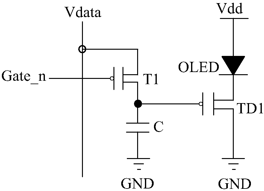
[0035] In order to make the purpose, technical solutions and advantages of the present invention clearer, the present invention will be further described in detail below in conjunction with the accompanying drawings. Obviously, the described embodiments are only some of the embodiments of the present invention, rather than all of them. Based on the design concepts of the embodiments of the present invention, all other embodiments obtained by those skilled in the art by replacing the type of transistors without creative efforts shall also fall within the protection scope of the present invention.

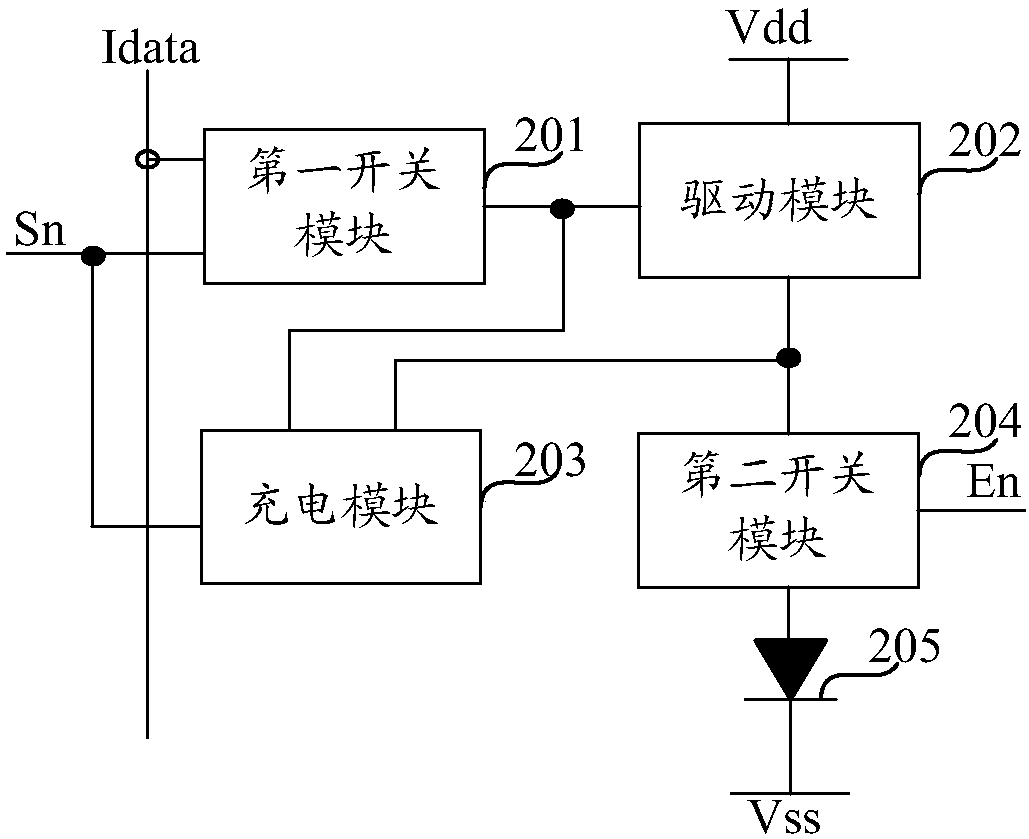
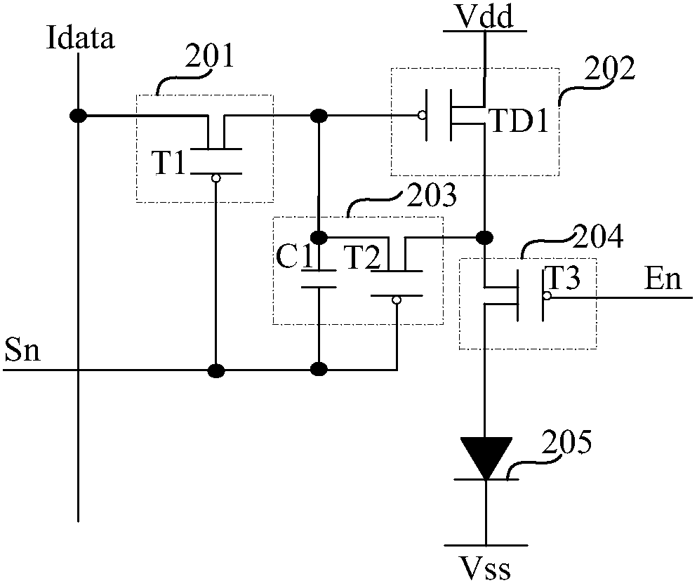
[0036] Such as figure 2 As shown, it is a schematic structural diagram of a pixel driving circuit provided by an embodiment of the present invention, including: a first switch module 201 , a drive module 202 , a charging module 203 , a second switch module 204 and an OLED 205 .

[0037] Specifically, the first terminal of the first switch module 201 is connected to the first scan co...


PUM


Abstract

The invention discloses an array substrate, a pixel driving circuit and a pixel driving method. The pixel driving circuit comprises a first switching module, a second switching module, a charging module, a driving module and an organic light-emitting diode (OLED), wherein the first switching module is used for outputting a current data signal to the driving module according to a first scanning control signal, the driving module is used for outputting driving current of the OLED to the second switching module according to the current data signal, and the charging module is used for charging theOLED. According to the embodiment of the invention, the charging time is reduced through charging the OLED by a high charging current source, and the final current is enabled to meet the current required by the OLED through circuit operations.

Description

technical field [0001] The invention belongs to the technical field of electronic circuits, and in particular relates to an array substrate, a pixel driving circuit and a pixel driving method. Background technique [0002] As a new generation of display technology, OLED (Organic Light Emitting Diode, Organic Light Emitting Diode) display has the advantages of low power consumption, high color gamut, high brightness, high resolution, wide viewing angle, high response speed, etc. application. [0003] figure 1 It is a pixel driving circuit diagram of an OLED display in the prior art, that is, a voltage-driven pixel driving circuit structure composed of two TFTs (Thin Film Transistor, thin film transistor) and a capacitor (ie, a 2T1C driving circuit structure). [0004] Wherein, Gate n is the scan control signal control line of the nth row, VData is the grayscale voltage signal line of the nth column, Vdd is the power supply voltage, and GND is the power supply ground. T1 is...

Claims


Application Information

Patent Timeline
Patent Type & Authority Applications(China)
IPC IPC(8): G09G3/3266G09G3/3225
CPCG09G3/3266G09G3/3225
Inventor 曾迎祥
Owner EVERDISPLAY OPTRONICS (SHANGHAI) CO LTD
Why Eureka
Try Eureka