Photovoltaic glass antireflection film
A technology of photovoltaic glass and anti-reflection film, applied in the coating and other directions, can solve the problems of increasing the length of the coating production line, narrow spectrum of the anti-reflection film, etc., to increase the length of the production line and the material and production cost, good color neutrality, good compatibility
- Summary
- Abstract
- Description
- Claims
- Application Information
AI Technical Summary
Problems solved by technology
Method used
Image
Examples
Embodiment 1
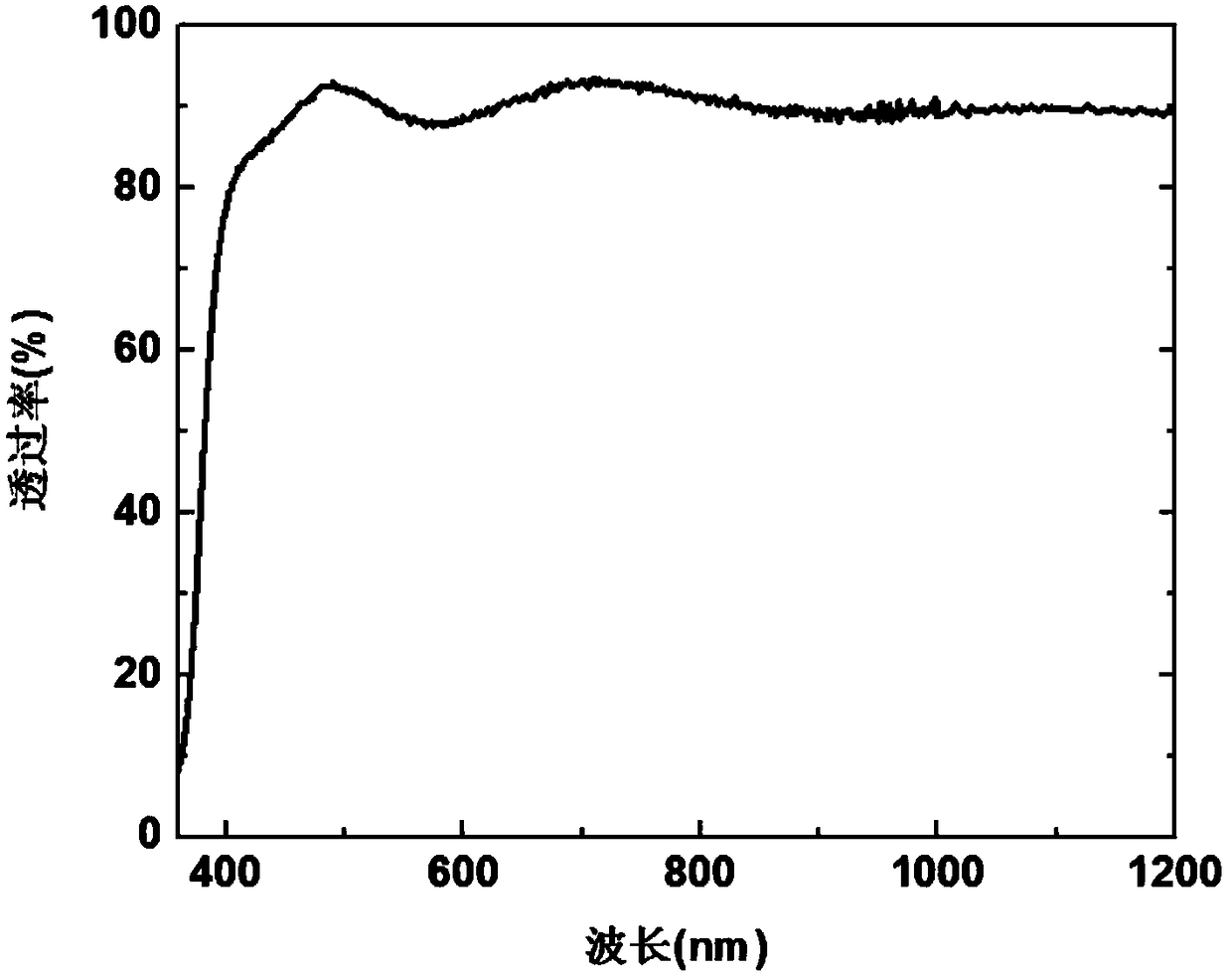
[0027] The photovoltaic glass anti-reflection film of embodiment 1, such as figure 1 As shown, it includes a glass substrate 10 and an anti-reflection film compounded on the surface of the glass substrate 10. The glass substrate 10 is ultra-white low-iron glass, and the anti-reflection film is a multilayer film prepared by reactive DC magnetron sputtering deposition. Layers of films are sequentially stacked on the surface of the glass substrate 10 from the inside to the outside, wherein the first layer 21 is Al 2 o 3 coating, the second layer 22 is SiO 2 coating, the third layer 23 is Al 2 o 3 coating, the fourth layer 24 is TiO 2 coating, the fifth layer 25 is SiO 2 coating, the sixth layer 26 is TiO 2 coating, the seventh layer 27 is SiO 2 plating.
[0028] In embodiment 1, the Al of the first layer 21 2 o 3 The thickness of the coating is 15nm, the second layer 22 of SiO 2 The thickness of the coating is 25nm, the Al of the third layer 23 2 o 3 The thickness of...
Embodiment 2
[0032] The difference between the photovoltaic glass antireflection film of embodiment 2 and embodiment 1 is that in embodiment 2, the glass substrate 10 is patterned glass, and the antireflection film is prepared on the patterned glass 10 by radio frequency magnetron sputtering, and ZnO coating instead of Al 2 o 3 Plating, with Nb 2 o 5 Coating instead of TiO 2 plating.
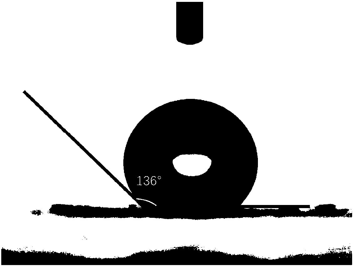
[0033] In Example 2, the monomolecular hydrophobic functional layer 30 was prepared on the surface of the antireflection film by vapor deposition of hexamethyldisilazane.
[0034] In embodiment 2, the thickness of the ZnO plating layer of the first layer 21 is 10nm, the SiO of the second layer 22 2 The thickness of the coating is 25nm, the thickness of the ZnO coating of the third layer 23 is 70nm, the Nb of the fourth layer 24 2 o 5 The thickness of the coating is 110nm, the fifth layer is 25 SiO 2 The thickness of the coating is 30nm, the sixth layer of 26 Nb 2 o 5 The thickness of the coating is...
PUM
| Property | Measurement | Unit |
|---|---|---|
| thickness | aaaaa | aaaaa |
| thickness | aaaaa | aaaaa |
| thickness | aaaaa | aaaaa |
Abstract
Description
Claims
Application Information
 - R&D
- Intellectual Property
- Life Sciences
- Materials
- Tech Scout
- Unparalleled Data Quality
- Higher Quality Content
- 60% Fewer Hallucinations
Browse by: Latest US Patents, China's latest patents, Technical Efficacy Thesaurus, Application Domain, Technology Topic, Popular Technical Reports.
© 2025 PatSnap. All rights reserved.Legal|Privacy policy|Modern Slavery Act Transparency Statement|Sitemap|About US| Contact US: help@patsnap.com


