USB interface circuit and mobile terminal
A USB interface and circuit technology, applied in the field of universal serial bus, can solve problems such as poor contact, ID contact corrosion, and inability to identify OTG devices.
- Summary
- Abstract
- Description
- Claims
- Application Information
AI Technical Summary
Problems solved by technology
Method used
Image
Examples
Embodiment 1
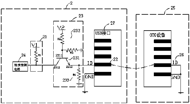
[0016] see figure 2 , is a schematic diagram of the principle of the USB interface circuit provided by an embodiment of the present invention.
[0017] The USB interface circuit of this embodiment includes a power circuit 21 , a USB interface 27 with an ID contact 22 , an isolation circuit 23 between the power circuit and the ID contact, and a trigger detection circuit 24 . The isolation circuit includes a first bias circuit 232, a second bias circuit 233, and a transistor 231. The control terminal 2311 of the transistor is electrically connected to the voltage output terminal of the first bias circuit, and the first terminal 2312 of the transistor is connected to the output terminal of the power supply circuit. Commonly electrically connected to the input terminal of the trigger detection circuit 24, the second terminal 2313 of the transistor and the voltage output terminal of the second bias circuit are commonly electrically connected to the ID contact. When the OTG device...
Embodiment 2
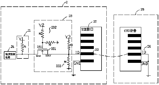
[0042] The difference between this embodiment and the first embodiment is that the transistor is changed from an NPN triode to an NMOS field effect transistor 331 . The control terminal 3311 of the transistor is the gate of the field effect transistor, the first terminal 3312 is the drain of the field effect transistor, and the second terminal 3313 is the source of the field effect transistor. In addition, the second bias circuit 333 is also different. Specifically, the second bias circuit includes a third power supply V3, and a fifth resistor R5 and a sixth resistor R6 connected in series between the third power supply and ground. The voltage output end of the setting circuit is the common end of the fifth resistor and the sixth resistor. In this embodiment, R5=100KΩ, R6=50KΩ, V3=V1=1.8V can be selected.
[0043] In this embodiment, R2=100KΩ and R3=150KΩ are selected, so that the output voltage of the voltage output end of the first bias circuit is 1.1V.
[0044] When the O...
PUM
 Abstract
Description
Claims
Application Information
 - Generate Ideas
- Intellectual Property
- Life Sciences
- Materials
- Tech Scout
- Unparalleled Data Quality
- Higher Quality Content
- 60% Fewer Hallucinations
Browse by: Latest US Patents, China's latest patents, Technical Efficacy Thesaurus, Application Domain, Technology Topic, Popular Technical Reports.
© 2025 PatSnap. All rights reserved.Legal|Privacy policy|Modern Slavery Act Transparency Statement|Sitemap|About US| Contact US: help@patsnap.com


