Buck type dc/dc converter circuit with anti-ringing block circuit
An anti-ringing and circuit technology, applied in the direction of output power conversion devices, instruments, electrical components, etc., can solve problems such as affecting the work of the chip, and achieve the effects of reducing chip area, reducing cost, and novel design
- Summary
- Abstract
- Description
- Claims
- Application Information
AI Technical Summary
Problems solved by technology
Method used
Image
Examples
Embodiment Construction
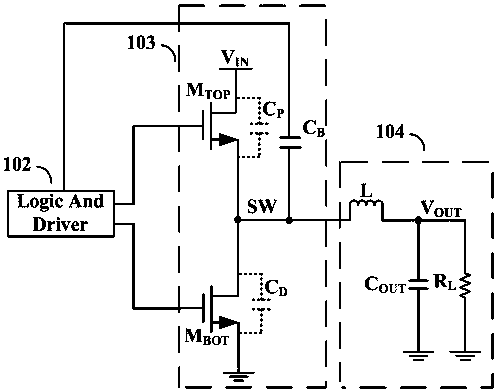
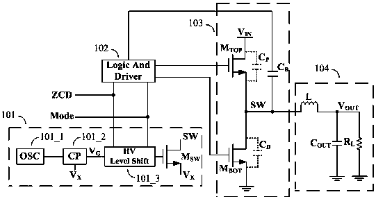
[0026] Such as figure 2 As shown, the Buck DC / DC converter circuit with anti-ringing module circuit includes at least: anti-ringing module circuit 101, logic drive circuit 102, power MOS tube 103, LC filter circuit and load 104, LC filter circuit and The load 104 is electrically connected to the output end of the power MOS tube 103, and the anti-ringing module circuit 101 is electrically connected to the power MOS tube 103 through the logic driving circuit 102.
[0027] The anti-ringing module circuit 101 and the logic drive circuit 102 at least include a zero-crossing comparison signal ZCD detection terminal and a mode selection signal Mode terminal that are electrically connected.
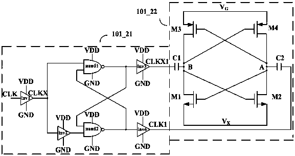
[0028] The anti-ringing module circuit 101 includes an oscillator clock module 101_1, a charge pump module 101_2, a high voltage level shift module 101_3, and a high voltage NMOS tube M SW The oscillator clock module 101_1, the charge pump module 101_2, the high voltage level shift module 101_3 and t...
PUM
 Abstract
Description
Claims
Application Information
 - R&D
- Intellectual Property
- Life Sciences
- Materials
- Tech Scout
- Unparalleled Data Quality
- Higher Quality Content
- 60% Fewer Hallucinations
Browse by: Latest US Patents, China's latest patents, Technical Efficacy Thesaurus, Application Domain, Technology Topic, Popular Technical Reports.
© 2025 PatSnap. All rights reserved.Legal|Privacy policy|Modern Slavery Act Transparency Statement|Sitemap|About US| Contact US: help@patsnap.com


