Electronic device test system and method thereof

An electronic device and test system technology, applied in the direction of electrical digital data processing, error detection/correction, and detection of faulty computer hardware, etc., can solve problems such as discarding, energy and labor costs, and misjudgment of the test system

Inactive Publication Date: 2018-07-31
PRIMAX ELECTRONICS LTD
View PDF5 Cites 0 Cited by
  • Summary
  • Abstract
  • Description
  • Claims
  • Application Information

AI Technical Summary

Problems solved by technology

However, if the electronic device is not properly connected to the test system at this time, it is easy to cause a misjudgment by the test system, so that the electronic device with normal function is judged as a defective product, and the electronic device with normal function becomes electronic waste and is discarded.
In addition, if the functional status of suspected defective products is confirmed for the second time, in addition to increasing the frequency of retesting of electronic devices by the testing system, more energy and labor costs are consumed, and it is also impossible to accurately control the operating performance of the production line

Method used


Image

  • Electronic device test system and method thereof
  • Electronic device test system and method thereof
  • Electronic device test system and method thereof

Examples


Embodiment Construction

[0041] The advantages and features of the present invention and methods for attaining the same will be more easily understood by more detailed description with reference to exemplary embodiments and accompanying drawings. However, the invention may be embodied in different forms and should not be construed as limited to the embodiments set forth herein. On the contrary, for those skilled in the art, these embodiments are provided to make this disclosure more thorough, comprehensive and fully convey the implementation of the present invention.

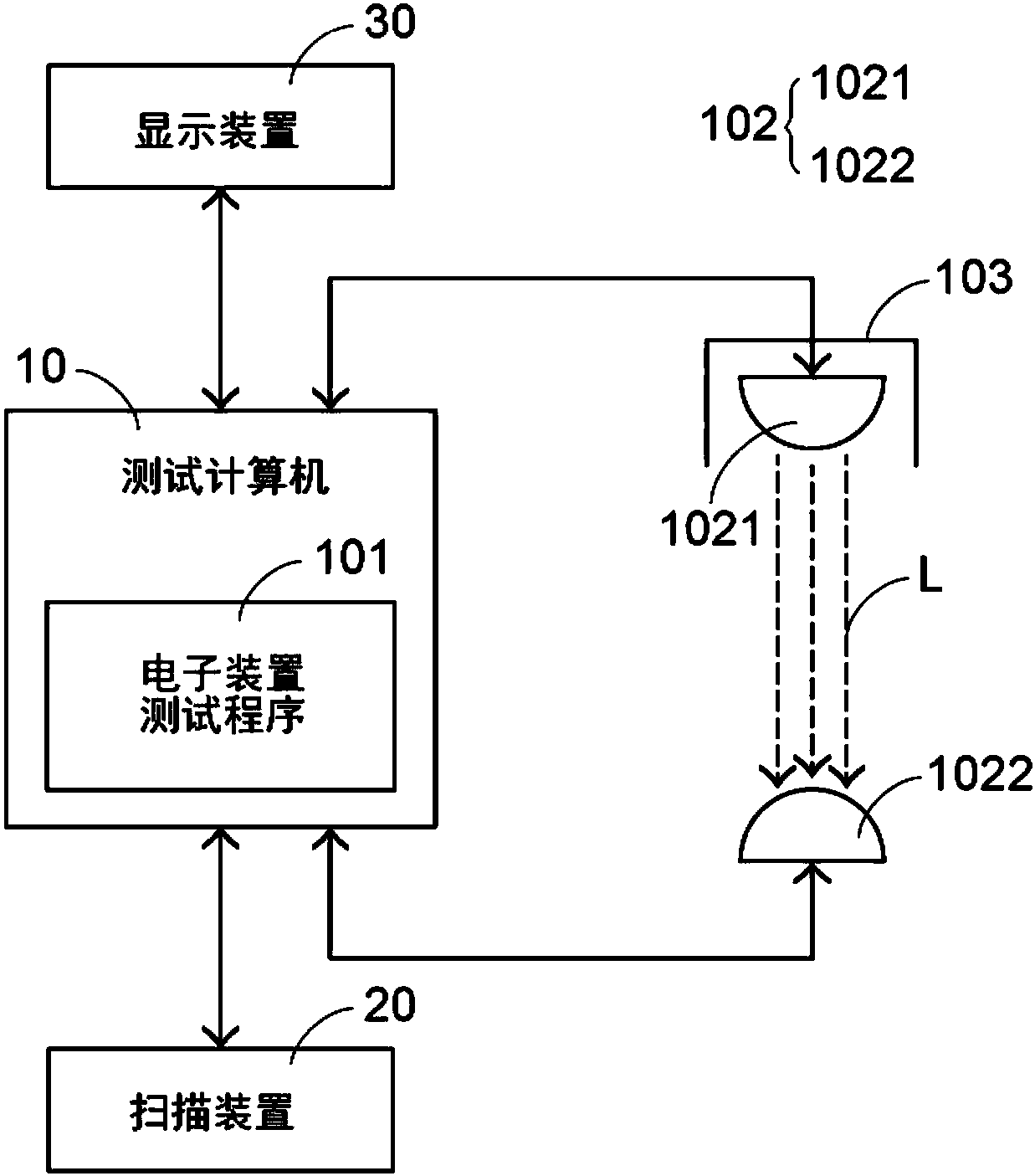
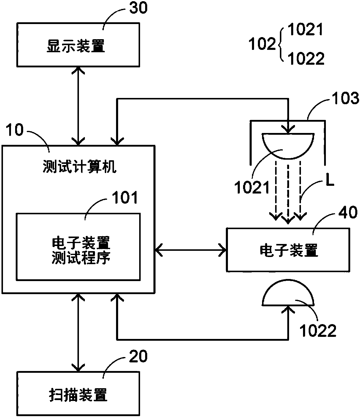
[0042] First, see Figure 1A and Figure 1B as shown, Figure 1A and 1B Test system for electronic devices. At Figure 1A and Figure 1B Among them, the electronic device testing system installed in the production line testing station includes: a testing computer 10 , a scanning device 20 and a display device 30 , wherein the testing computer 10 is electrically connected to the scanning device 20 and the display device 30 .

[0043]...


PUM


Abstract

The invention provides an electronic device test system and a method thereof. The electronic device test system is used for testing functions of an electronic device. The electronic device test systemcomprises a test computer, a scanning device and a light sensing module, wherein the test computer is used for executing an electronic device test program; the scanning device is used for scanning abarcode number of the electronic device; the light sensing module is used for detecting a connection state between the electronic device and the test computer; and when the light sensing module confirms the connection state, the electronic device test program starts a test function to test the electronic device, a test result of the electronic device is recorded according to the barcode number, and a re-test rate is generated according to the test result.

Description

technical field [0001] The invention relates to an application field of electronic device testing, in particular to an electronic device testing system with connection confirmation and a method thereof. Background technique [0002] Electronic devices and related products have become an integral part of human society. Hundreds of millions of electronic products are sold around the world every year, including laptops, tablets, personal digital assistants, mobile phones, etc. With the growth of mass consumption and the advancement of science and technology, the speed of replacing old and new electronic products is getting faster and faster, and the resulting electronic waste is also causing great harm to the global environment. [0003] In order to reduce the total amount of electronic waste, on the consumer side, the functionality and diversity of electronic products can be increased to reduce the rate at which consumers replace electronic products; on the production side, th...

Claims


Application Information

Patent Timeline
Patent Type & Authority Applications(China)
IPC IPC(8): G06F11/22
CPCG06F11/2221G06F11/2268
Inventor 张倍铭许世杰张世杰黄伟隆
Owner PRIMAX ELECTRONICS LTD
Why Eureka
Try Eureka