
Method and system for testing eMMC chip storage parameters

A parameter test and chip technology, applied in static memory, instruments, etc., can solve problems such as difficulty in replacement, trouble, and failure to reach the limit life of eMMC chips, and achieve long-term reliability and faster detection speed.

Active Publication Date: 2018-07-10
重庆金山医疗技术研究院有限公司
View PDF4 Cites 4 Cited by
  • Summary
  • Abstract
  • Description
  • Claims
  • Application Information

AI Technical Summary

Problems solved by technology

When eMMC chips are used in digital products such as mobile phones and TVs, since the frequency of reading operations for these products is much higher than that of writing operations for eMMC chips during use, the service life of eMMC chips is very long. In addition, digital products The update is very fast, and the service life limit of the eMMC chip is basically not reached; however, if the eMMC chip is used for portable data storage and recording equipment, especially for a recorder that records a large amount of data in real time, the frequency of writing operations is very high , and this type of product has very high requirements on the integrity and reliability of data, and a set of equipment has a long service life and will not be updated frequently. The eMMC chip is difficult and troublesome to replace due to the characteristics of the BGA package. Therefore, equipment manufacturers are designing products. When testing products, performance, read and write life tests must be performed on the selected eMMC chips
[0005] At present, the evaluation of eMMC chip performance and life indicators is mostly based on the data manual provided by the chip manufacturer, and the relevant test and verification methods are only known to the chip manufacturer itself; there are also senior digital companies or players who use some limit testing software for PC platform SSD ( Main control chip + multi-chip NAND FLASH) for life test, but because of different platform systems, etc., it is not suitable for eMMC chip evaluation

Method used

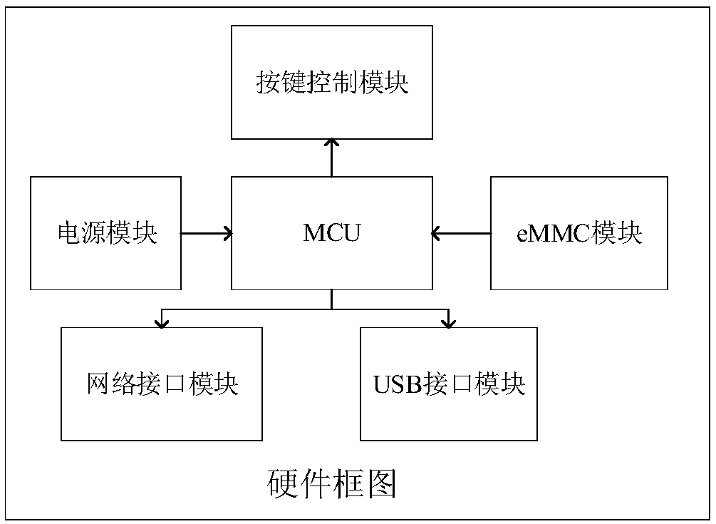
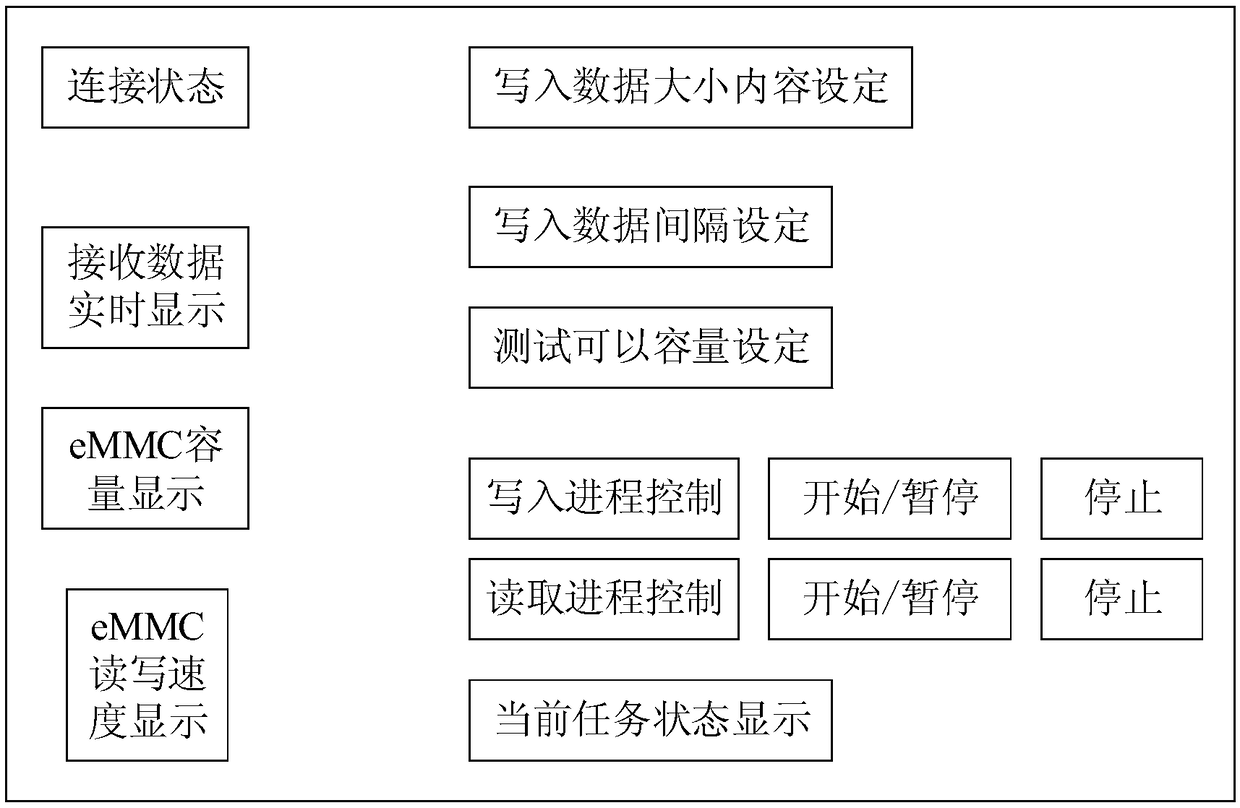

Image

  • Method and system for testing eMMC chip storage parameters
  • Method and system for testing eMMC chip storage parameters
  • Method and system for testing eMMC chip storage parameters

Examples


Embodiment Construction

[0054] Embodiments of the present invention are described in detail below, examples of which are shown in the drawings, wherein the same or similar reference numerals designate the same or similar elements or elements having the same or similar functions throughout. The embodiments described below by referring to the figures are exemplary only for explaining the present invention and should not be construed as limiting the present invention.

[0055] In describing the present invention, it should be understood that the terms "longitudinal", "transverse", "upper", "lower", "front", "rear", "left", "right", "vertical", The orientation or positional relationship indicated by "horizontal", "top", "bottom", "inner", "outer", etc. are based on the orientation or positional relationship shown in the drawings, and are only for the convenience of describing the present invention and simplifying the description, rather than Nothing indicating or implying that a referenced device or elem...


PUM


Abstract

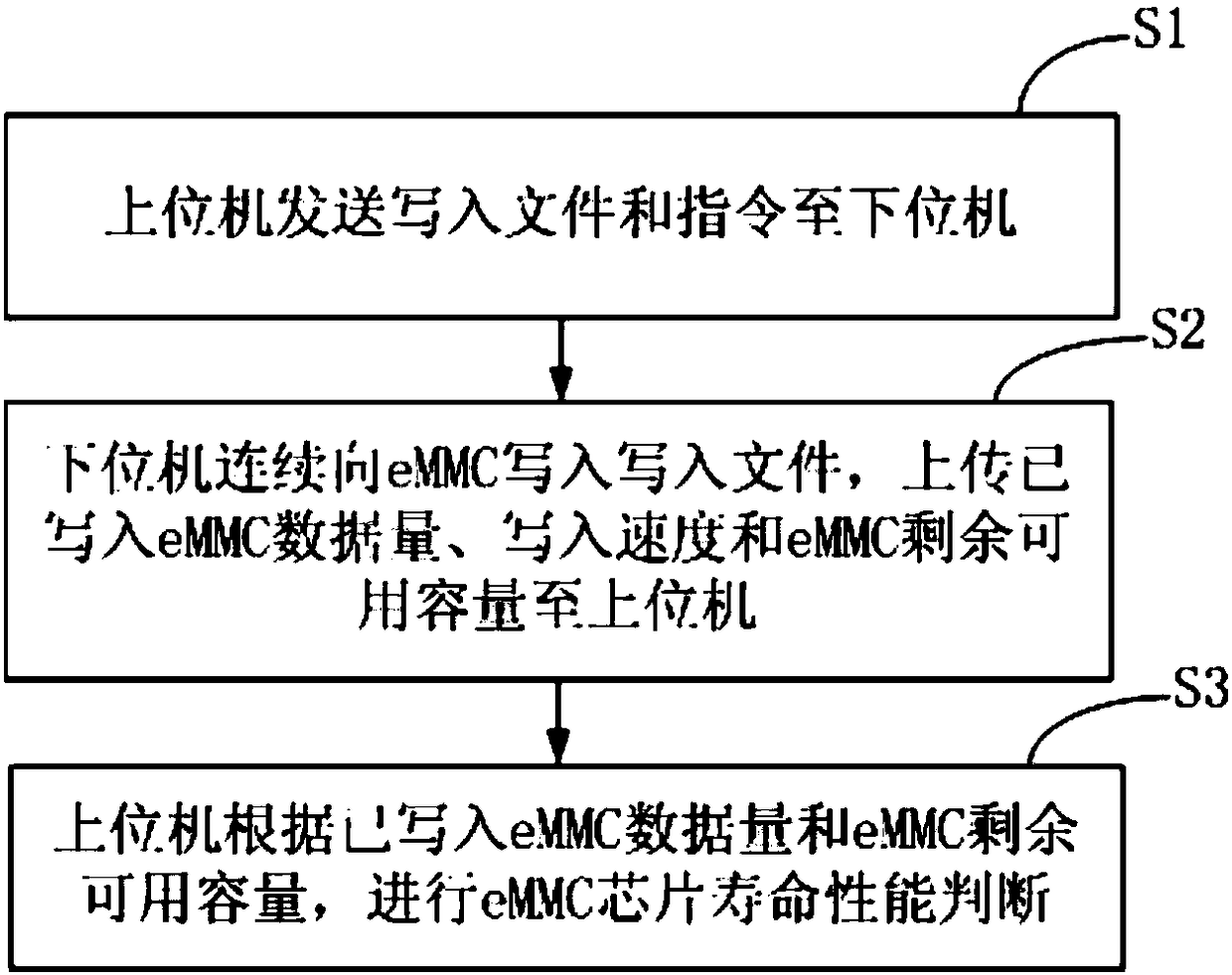
The invention discloses a method and system for testing eMMC chip storage parameters. The method comprises S1, transmitting a writing file and an instruction to a lower computer through an upper computer, S2, writing the instruction through the lower computer, and S3, determining the life of an eMMC chip through the upper computer, wherein when the eMMC chip is full, if the remaining available capacity of the eMMC chip reaches the amount of stored data in a single detection process and the written eMMC chip data amount is greater than or equal to the estimated total capacity of the manufacturer, the life of the eMMC chip satisfies the requirements, and otherwise, the life of the eMMC chip dies not satisfy the requirements. When the eMMC chip is used in a real-time mass data storage recorder, the manufacturer can conveniently and fast detect and assess the performances and life of the eMMC chip through the method and system. The system can be used as a reliable test tool, guarantee theuse reliability and long life of the product and evaluate eMMC chips with different capacities.

Description

technical field [0001] The invention relates to a storage chip testing method, in particular to a method and system for testing eMMC chip storage parameters. Background technique [0002] The eMMC chip (Embedded Multi Media Card, embedded multimedia card) is composed of NAND Flash, a controller and a standard packaging interface. Among them, NAND Flash provides storage space; the controller realizes the read and write control and management of Flash blocks, including ECC Error correcting code, block management, wear leveling, command management, low power management, etc.; standard package interface realizes multi- The different read and write instructions of branded NAND Flash are unified in the user interface, so that users can focus on application development without having to consider the differences in Flash brands and processes. The eMMC chip is packaged with BGA (BallGrid Array Package) technology, and circular or columnar solder joints are distributed under the pack...

Claims


Application Information

Patent Timeline
Patent Type & Authority Applications(China)
IPC IPC(8): G11C29/56
CPCG11C29/56G11C2029/5604
Inventor 冉亮田维明张志良彭林刘江
Owner 重庆金山医疗技术研究院有限公司
Learn More