Display apparatus and method and apparatus for manufacturing the same

A display device and display surface technology, applied in nonlinear optics, instruments, optics, etc., can solve problems such as insufficient correction of bright spot defects, light leakage, and thinning of the scanning part, and achieve the effect of suppressing bright spot defects

Active Publication Date: 2018-07-06
PANASONIC INTELLECTUAL PROPERTY MANAGEMENT CO LTD
View PDF10 Cites 0 Cited by
  • Summary
  • Abstract
  • Description
  • Claims
  • Application Information

AI Technical Summary

Problems solved by technology

[0008] However, in the prior art, when the colored layer is formed by surface scanning of laser light, the final scanning part becomes thinner, light leakage occurs, and defects due to bright spot defects cannot be sufficiently corrected.

Method used


Image

  • Display apparatus and method and apparatus for manufacturing the same
  • Display apparatus and method and apparatus for manufacturing the same
  • Display apparatus and method and apparatus for manufacturing the same

Examples


Embodiment approach 1

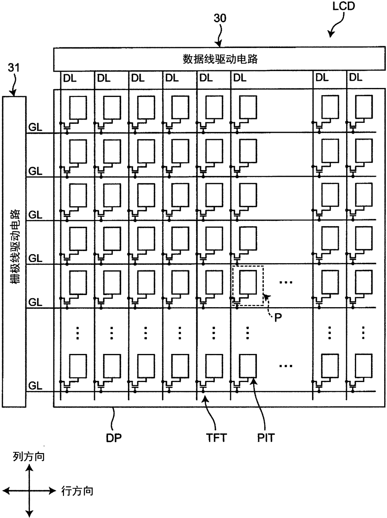
[0099] figure 1 It is a plan view showing the overall configuration of a liquid crystal display device LCD as an example of the display device according to Embodiment 1 of the present invention.

[0100] The liquid crystal display device LCD includes: a display panel DP for displaying images, a display panel drive circuit (data line drive circuit 30, gate line drive circuit 31) for driving the display panel DP, a control circuit (not shown) for controlling the display panel drive circuit. ) and a backlight 134 that illuminates the backlight that irradiates light to the display panel DP from the rear side.

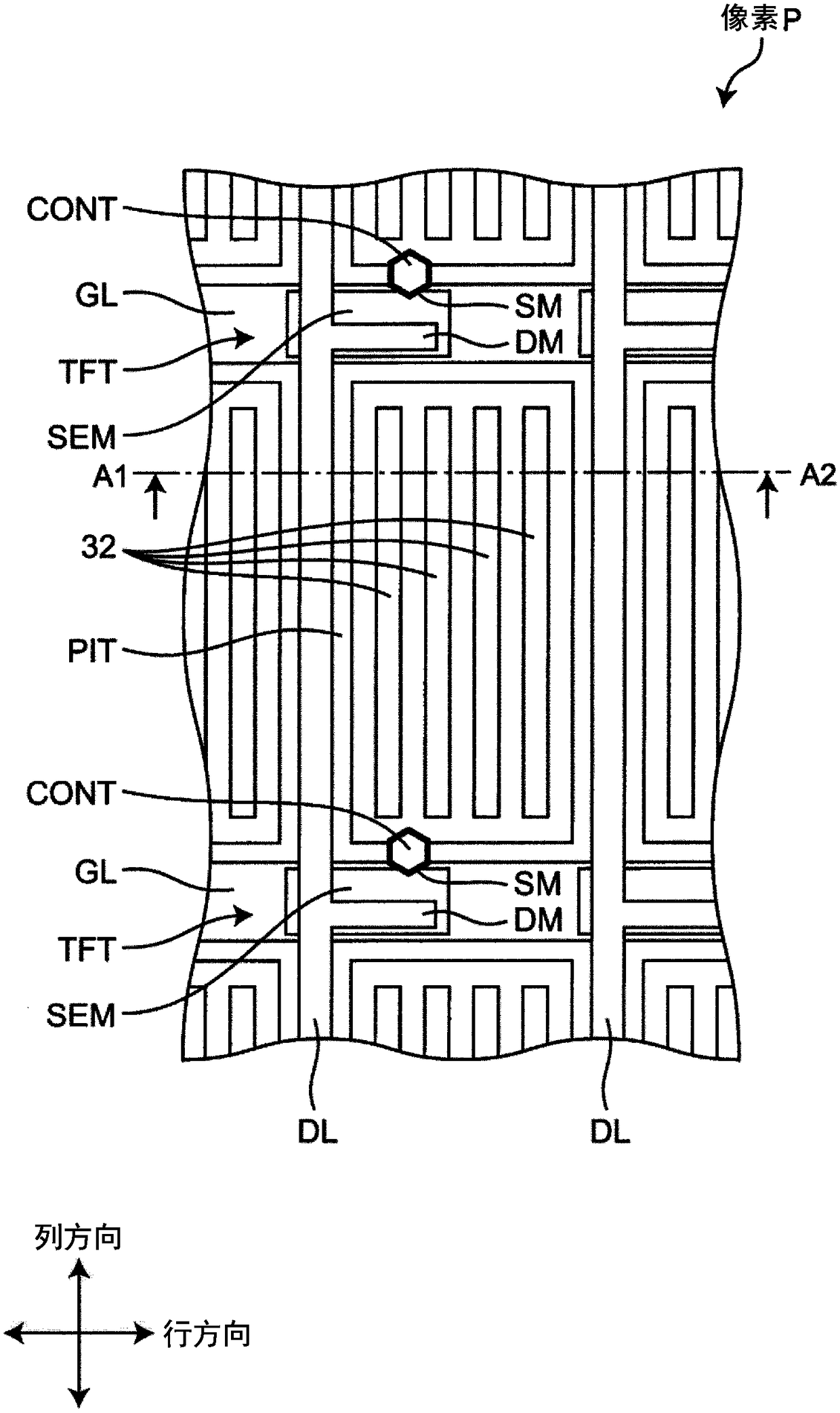
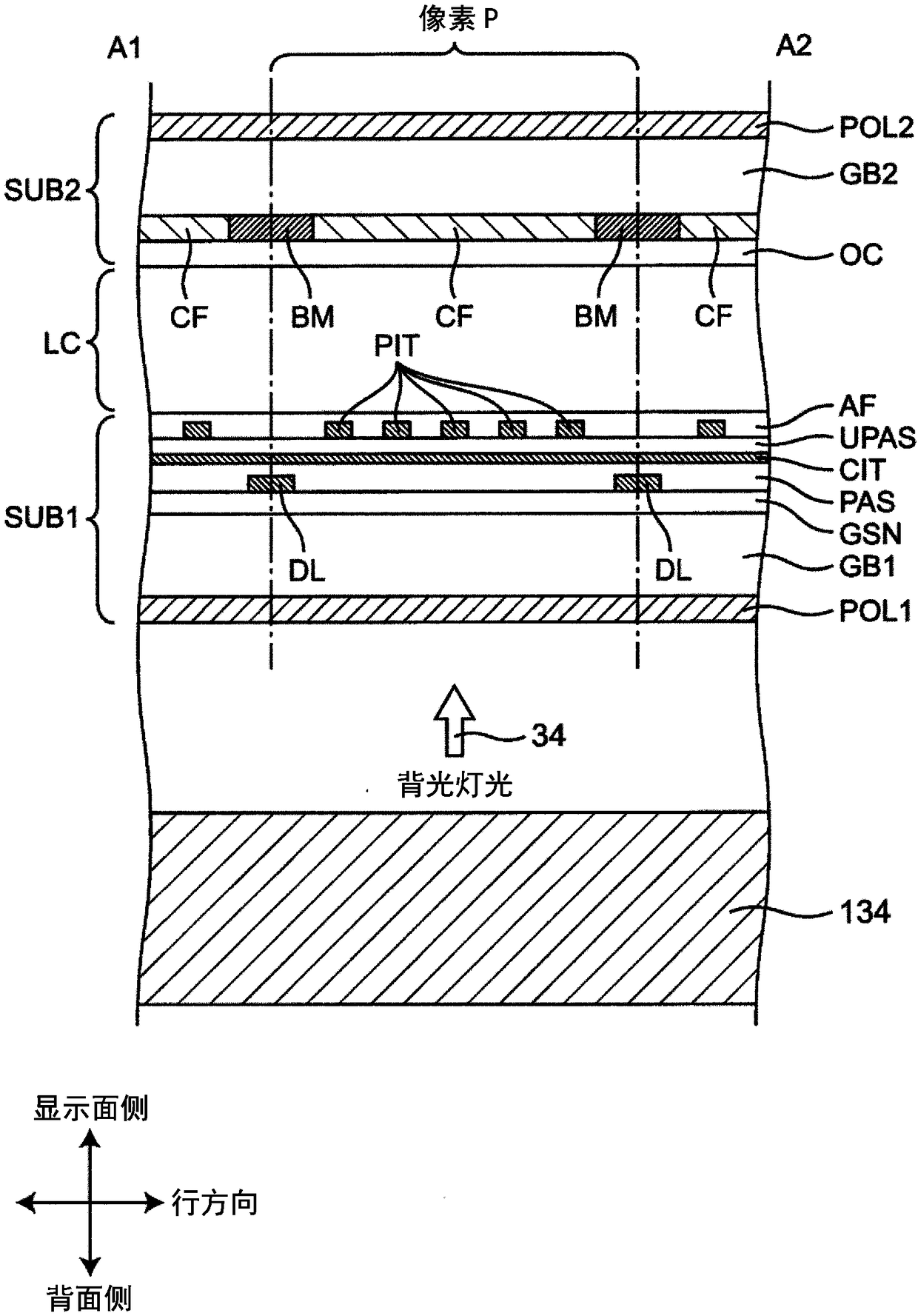
[0101] figure 2 It is a plan view showing the configuration of a part of the display panel DP. image 3 is in figure 2 The end view of the cut section cut at the line A1-A2 of . In addition, in figure 2 as well as image 3 , represents a pixel P in the display panel DP.

[0102] Such as image 3 As shown, the display panel DP includes: a thin film transistor subs...


PUM

PropertyMeasurementUnit
wavelengthaaaaaaaaaa

Abstract

The present invention provides a display device, a method and apparatus for manufacturing the same, capable of suppressing degradation of display quality caused by bright spot defects. A display device (LCD) includes a first glass substrate (SUB1) and a second glass substrate (SUB2) that faces the first glass substrate and is located on a display surface side; a dimming portion (1) that covers thebright spot defect portion (133) as viewed from the display surface side is arranged inside at least one of the first glass substrate and the second glass substrate; the dimming portion has a lineartransmissive portion (7) having the transmittance of visible light higher than that of the other region (1 g) of the dimming portion as viewed from the display surface side; a cross section of the dimming portion in the thickness direction orthogonal to the longitudinal direction of the linear transmissive portion is in a folding line shape where a plurality of colored layers (2-1, 2-2) are continuous and bent, and the transmissive portion is located at the bent end portion (47) of the folding line.

Description

technical field [0001] The present invention relates to a display device, a manufacturing method thereof, and a manufacturing device. Background technique [0002] Among various display devices, for example, a liquid crystal display device drives the liquid crystal by applying an electric field generated between the pixel electrode and the common electrode to the liquid crystal layer sandwiched by a pair of substrates, thereby adjusting the transmission between the pixel electrode and the common electrode. The amount of light in the area for image display. [0003] Conventionally, for example, in liquid crystal display devices, there has been known a problem of so-called bright spot defects (also referred to as pixel defects) in which the display luminance of pixels is higher than desired. The bright spot defect occurs, for example, when a foreign matter is mixed between a pair of substrates during the manufacturing process of a liquid crystal display device, and the alignm...

Claims


Application Information

Patent Timeline
Patent Type & Authority Applications(China)
IPC IPC(8): G02F1/13G02F1/1333G02F1/1335
CPCG02F1/1309G02F1/1333G02F1/1335G02F1/133302G02F1/133516G02F1/133512G02F1/133519
Inventor 北村嘉朗森重之
Owner PANASONIC INTELLECTUAL PROPERTY MANAGEMENT CO LTD
Why Eureka
Try Eureka