Gate driver monolithic (GDM)
A driving circuit and gate scanning technology, which is applied in the direction of instruments and static indicators, etc., can solve the problems of weak maintenance ability of the driving circuit unit, false opening of the scanning signal Gn, and influence on the pull-up control node, so as to save layout space and improve Circuit reliability, effect of preventing narrowing of signal pulse width
- Summary
- Abstract
- Description
- Claims
- Application Information
AI Technical Summary
Problems solved by technology
Method used
Image
Examples
Embodiment 1
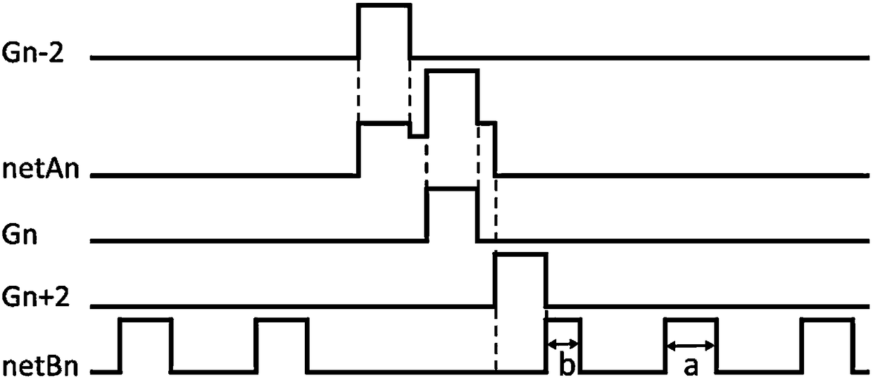
[0062] Such as Figure 6 Shown is a circuit diagram of Embodiment 1 of a gate scanning drive circuit, the nth level drive circuit unit includes a pull-up control module 1, a pull-up module 2, a maintenance control node generation module 3, a pull-up control node maintenance module 4, The output node maintains the module 5 and the bootstrap capacitor C1.
[0063]The pull-up control module 1, the pull-up module 2, the maintenance control node generation module 3 and the pull-up control node maintenance module 4 are connected to the pull-up control node netAn; the maintenance control node generation module 3, the pull-up control node maintenance module 4 and the output The node maintenance modules 5 all input low-level VSS; the pull-up module 2 and the output node maintenance module 5 are connected to the scanning signal line of the current stage, and the scanning signal line outputs the scanning signal Gn; the maintenance control node generation module 3 and the pull-up control ...
Embodiment 2
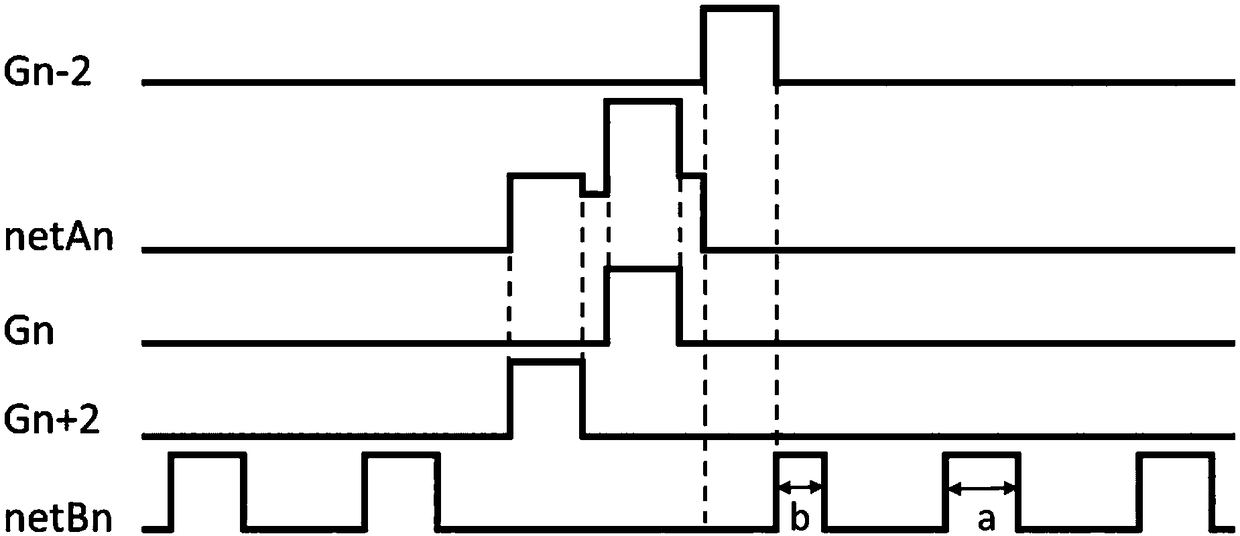
[0108] Figure 9 It is a schematic circuit diagram of Embodiment 2 of a gate scanning driving circuit of the present invention. The second embodiment is improved on the basis of the first embodiment, and the specific improvements are as follows:
[0109] The sustain control node generation module 3 further includes a fourteenth thin film transistor M6A and a fifteenth thin film transistor M6B.
[0110] The control terminal of the fourteenth thin film transistor M6A inputs the first control signal, and the two pass terminals of the fourteenth thin film transistor M6A are respectively connected to the sustain control node netBn of the nth driver circuit unit and the reverse scan control signal D2U. The fourteenth thin film transistor M6A is used to prohibit and maintain the output of the control node netBn during the working period of the n-2th stage circuit unit in the forward scan process, that is, during the precharge phase of the forward scan.
[0111] The control terminal...
PUM
 Abstract
Description
Claims
Application Information
 - Generate Ideas
- Intellectual Property
- Life Sciences
- Materials
- Tech Scout
- Unparalleled Data Quality
- Higher Quality Content
- 60% Fewer Hallucinations
Browse by: Latest US Patents, China's latest patents, Technical Efficacy Thesaurus, Application Domain, Technology Topic, Popular Technical Reports.
© 2025 PatSnap. All rights reserved.Legal|Privacy policy|Modern Slavery Act Transparency Statement|Sitemap|About US| Contact US: help@patsnap.com


