Transistor device

A transistor and semiconductor technology, applied in semiconductor devices, electrical components, circuits, etc., can solve problems such as conductivity changes, on-voltage shifts, poor operational stability of electronic components, and avoid stress concentration effects.

Active Publication Date: 2020-09-25
HANNSTAR DISPLAY CORPORATION
View PDF26 Cites 0 Cited by
  • Summary
  • Abstract
  • Description
  • Claims
  • Application Information

AI Technical Summary

Problems solved by technology

Many semiconductor materials may change their conductivity (or semiconducting properties) after being stressed, which leads to poor operational stability of electronic components
For example, a transistor element using semiconductor material as a channel layer may experience a shift in the conduction voltage (or threshold voltage) or a phenomenon of leakage current after being stressed.

Method used


Image

  • Transistor device
  • Transistor device
  • Transistor device

Examples


Embodiment Construction

[0030] Reference will now be made in detail to the exemplary embodiments of the invention, examples of which are illustrated in the accompanying drawings. Wherever possible, the same reference numbers have been used in the drawings and description to refer to the same or like parts.

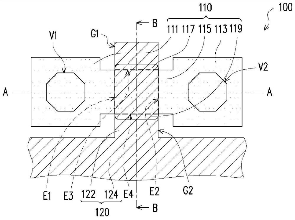
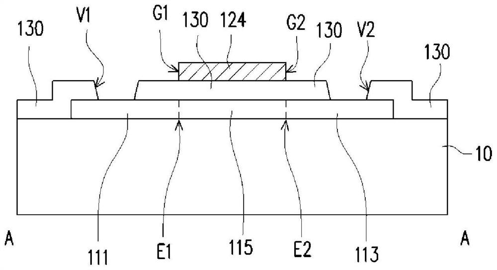
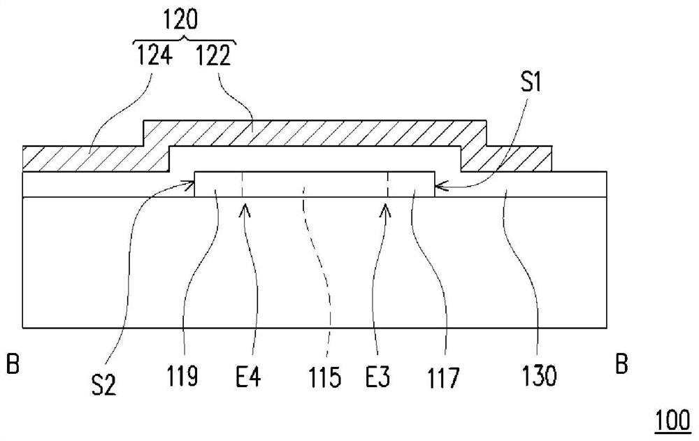
[0031] figure 1 is a schematic top view of a transistor device according to an embodiment of the present invention, figure 2 for figure 1 A schematic cross-section of the line A-A, image 3 for figure 1 Schematic cross-section of line B-B. Please also refer to Figure 1 to Figure 3 , the transistor device 100 may be disposed on the substrate 10 as an element having a switching function. The transistor structure 100 includes a semiconductor material layer 110 , a gate layer 120 and an insulating layer 130 . The semiconductor material layer 110 can be directly disposed on the substrate 10 , however, in other embodiments, other film layers, such as a buffer layer, can exist between the semic...


PUM


Abstract

The invention provides a transistor device comprising a semiconductor material layer, a gate layer and an insulating layer. The semiconductor material layer integrally includes a first conductive part, a second conductive part, a channel part and a first protruding part. The channel part is located between the first conductive part and the second conductive part. The channel part has a first boundary, a second boundary, a third boundary and a fourth boundary, wherein the first boundary is adjacent to the first conductive part, the second boundary is adjacent to the second conductive part, and the third boundary is connected to the fourth boundary. The endpoints of the first boundary and the second boundary. The first protruding portion protrudes outward from the third boundary of the channel portion. The gate layer traverses and overlaps the channel portion. The first gate boundary and the second gate boundary of the gate layer are overlapped with the first boundary and the second boundary of the channel part. The insulating layer is disposed between the gate layer and the semiconductor material layer.

Description

technical field [0001] The present invention relates to an electronic component, and in particular to a transistor device. Background technique [0002] With the development of manufacturing technology of electronic components, the research and development of flexible electronic products has become more and more vigorous. The main problem that flexible electronic products, such as flexible display panels, must overcome is that the electronic product will be continuously bent during use, so that components in the electronic product may be easily damaged due to the application of stress. Especially in electronic components, in order to realize the performance of the product, it is necessary to use semiconductor materials. Many semiconductor materials may change their electrical conductivity (or semiconductor properties) after being subjected to stress, which leads to poor operational stability of electronic components. For example, a transistor element using semiconductor ma...

Claims


Application Information

Patent Timeline
Patent Type & Authority Patents(China)
IPC IPC(8): H01L29/78H01L29/06H01L29/10H01L29/423
CPCH01L29/0684H01L29/1033H01L29/4232H01L29/78H01L29/78696H01L29/78675H01L29/66757H01L29/42384H01L29/41733H01L29/49
Inventor 王泰瑞张祖强冯捷威颜劭安陈韦翰
Owner HANNSTAR DISPLAY CORPORATION
Why Eureka
Try Eureka