


Quick Research
Generate reliable direction feasibility study reports for your R&D in just a few steps.

Technical Q&A
Discover and master advanced knowledge NOW. Basics, ideas, possibilities, all at once.

Find Solutions
As an expert in R&D theories, this can generate solutions to your technical problems instantly.

Evaluate Feasibility
Analyze your overall solution with one click, know your potential R&D risks in advance.

Monitor Landscape
Get weekly tech updates, stay abreast of the latest tech innovations and key insights.
High-efficiency organic fluorescent light emitting diode (LED) and preparation method thereof
A light-emitting diode and organic technology, applied in semiconductor/solid-state device manufacturing, electrical components, electric solid-state devices, etc., can solve the problems of complex device structure, difficulty in controlling doping concentration, etc., and achieve simple device structure, less preparation process, Effect of reducing material cost
- Summary
- Abstract
- Description
- Claims
- Application Information
AI Technical Summary
Problems solved by technology
Method used
Image


Examples
Embodiment 1
[0046] Take a number of ITO conductive glass substrates with the same batch number, the size is 30 mm × 30 mm, the thickness of ITO is about 90 nanometers, and the square resistance is about 20 ohms / square. Sequentially use acetone, special detergent for micron semiconductors, deionized water, and isopropanol to ultrasonically clean for 15 minutes to remove dirt on the surface of the substrate, and then put it in a constant temperature box for drying at 75 degrees Celsius for use. The dried ITO substrate was treated with plasma ignition equipment for 4 minutes to further remove the organic pollutants attached to the surface. Then the ITO substrate was transferred to an anhydrous and oxygen-free glove box filled with high-purity nitrogen. In this glove box, load the device into a vacuum evaporation chamber. Turn on the mechanical pump and molecular pump, when the evaporation chamber reaches 4×10 -4After a high vacuum of Pascal begins the thermal evaporation of the thin film. ...
Embodiment 2
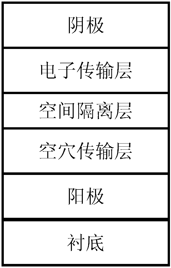
[0053] The preparation process is the same as that in Example 1, but the doped fluorescein is replaced by DCJTB, the doping concentration is still 1%, and the thickness of the space isolation layer mCP is respectively 0, 1, 2, and 3 nanometers. The obtained device structure is: ITO glass substrate / TAPC (70 nm) / DCJTB doped TAPC (15 nm) / space isolation layer mCP (0, 1, 2, 3 nm) / TmPyTZ (85 nm) / lithium fluoride (1 nm) / Al.
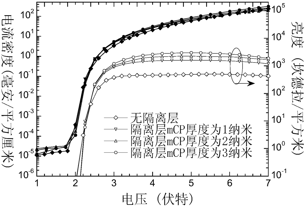
[0054] The organic fluorescent light-emitting diode obtained in this embodiment: ITO glass substrate / TAPC (70 nanometers) / DCJTB doped TAPC (15 nanometers) / space isolation layer mCP (0, 1, 2, 3 nanometers) / TmPyTZ (85 nanometers) The current density-brightness-voltage characteristic curve, the external quantum efficiency-current density characteristic curve and the electroluminescence spectrum at different current densities of / lithium fluoride (1 nanometer) / aluminum are respectively Figure 6 , Figure 7 and Figure 8 shown. in Figure 8 In (a), (b), (c), a...
PUM
 Abstract
Description
Claims
Application Information
 - R&D Engineer
- R&D Manager
- IP Professional
- Industry Leading Data Capabilities
- Powerful AI technology
- Patent DNA Extraction
Browse by: Latest US Patents, China's latest patents, Technical Efficacy Thesaurus, Application Domain, Technology Topic, Popular Technical Reports.
© 2024 PatSnap. All rights reserved.Legal|Privacy policy|Modern Slavery Act Transparency Statement|Sitemap|About US| Contact US: help@patsnap.com