High-pixel LED display module

A display module and high-pixel technology, applied in identification devices, instruments, light guides, etc., can solve problems such as low yield, difficult maintenance, and difficulty in making small-pitch display screens, and achieve the effect of increasing pixels and improving pixels

Inactive Publication Date: 2018-06-12
HUIZHOU THORLED OPTO
View PDF5 Cites 2 Cited by
  • Summary
  • Abstract
  • Description
  • Claims
  • Application Information

AI Technical Summary

Problems solved by technology

When producing high-pixel displays, the density of light-emitting points increases, and the number of bracket pins that need to be soldered increases. The difficulty of soldering is also due to the reduction of pins and the increase in number, resulting in low yield and difficult maintenance. It is difficult to meet the needs of small-pitch display screens.

Method used


Image

  • High-pixel LED display module
  • High-pixel LED display module
  • High-pixel LED display module

Examples


Embodiment 1

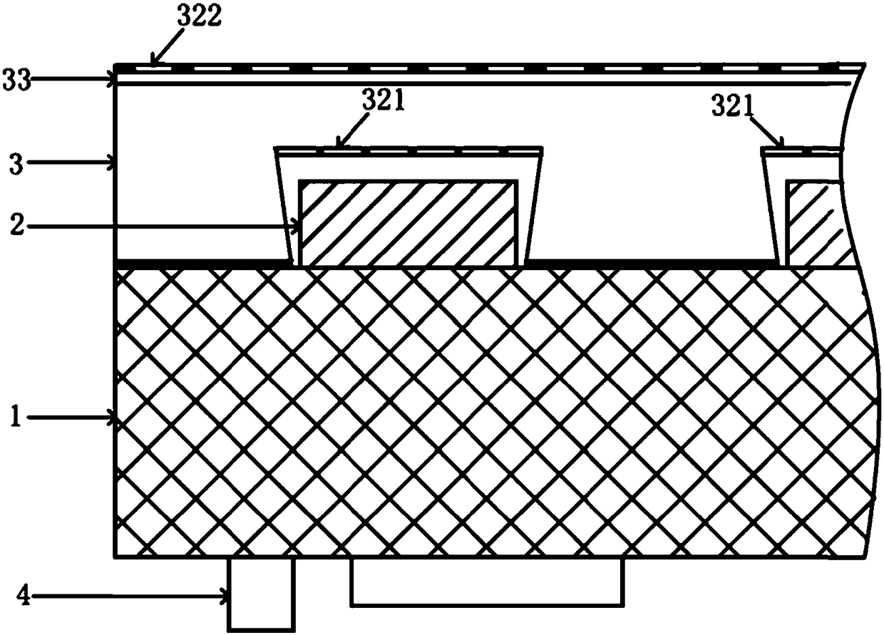
[0042] Such as figure 1 As shown, a high pixel LED display module includes a circuit substrate 1 , a light source 2 mounted on the circuit substrate 1 , a light guide layer 3 covering the circuit substrate 1 and an integrated circuit 4 mounted on the circuit substrate 1 . In this embodiment, the light source is an LED chip. The light source 2 emits light, and the light guide layer 3 guides the light emitted by the light source 2 to the outside of the light guide layer 3 . In this embodiment, the circuit substrate 1 can be composed of BT, FR4, ceramics, metal and other materials alone or in combination; the light source 2 can be a flip chip, a front chip or a vertical chip; the light guide layer 3 is a high temperature resistant material, such as acrylic, etc. .

[0043] Such as figure 1 , as shown in 2, a light source accommodating groove 31 for accommodating the light source 2 is provided on one surface of the light guide layer 3 close to the circuit substrate 2 . Such as...

Embodiment 2

[0067] The difference between the present embodiment and the first embodiment is that the light guide mechanism is a through hole arranged in the light guide layer to allow light to pass through. Light emitted by light sources of different colors passes through the through hole and is emitted to the outside of the light guide layer.

Embodiment 3

[0069] The difference between the present embodiment and the first embodiment is that the light sources all emit light of the same color. A red light filter, a green light filter and a blue light filter are respectively arranged in the different light guiding mechanisms. The red light filter, the green light filter and the blue light filter respectively absorb light of other colors in the light emitted by the light source, and only allow red light, green light and blue light to pass through.

[0070] In this embodiment, the red light filter, the green light filter and the blue light filter are respectively arranged in different light output ends.

[0071] In another embodiment, the red light filter, the green light filter and the blue light filter are respectively arranged in different lighting ends.


PUM


Abstract

The invention discloses a high-pixel LED display module, which comprises a circuit substrate, power sources and a light guide layer. The light sources are mounted on the circuit substrate, the light guide layer covers the circuit substrate and is provided with power source holding grooves and a plurality of light guide mechanisms, the power source holding grooves are used for holding the power sources, and the light guide mechanisms are used for transmitting light rays emitted by the light sources to the outside of the light guide layer. The invention further discloses a display screen with the high-pixel LED display module. By the light guide mechanisms for transmitting light rays emitted by the light sources to the outside of the light guide layer, high-pixel LED display is realized without reducing light source size and increasing light source distribution density.

Description

technical field [0001] The invention relates to the technical field of LED display, in particular to a high pixel LED display module. Background technique [0002] The LED display is a flat-panel display, which is composed of small LED module panels and is used to display various information such as text, images, videos, and video signals. [0003] Existing LED displays often adopt SMD display packaging technology, that is, SMD will be mounted on the circuit substrate of the display module by SMD technology. When producing high-pixel displays, the density of light-emitting points increases, and the number of bracket pins that need to be soldered increases. The difficulty of soldering is also due to the reduction of pins and the increase in number, resulting in low yield and difficult maintenance. It is difficult to meet the needs of small-pitch display screens. . Contents of the invention [0004] The object of the present invention is to provide a high-pixel LED display...

Claims


Application Information

Patent Timeline
IPC IPC(8): G09F9/33
CPCG09F9/33G02B6/0068G02B6/0021G02B6/0091
Inventor 陈锐冰罗锦长许晋源
Owner HUIZHOU THORLED OPTO
Why Eureka
Try Eureka