Semiconductor wafer electro-deposition method and semiconductor wafer electro-deposition device

An electrodeposition device, semiconductor technology, applied in the direction of semiconductor devices, circuits, electrolytic components, etc., can solve the problems of lower production efficiency, deposition layer color, abnormal appearance and quality of deposition layer, etc., to improve uniformity and eliminate electrodeposition edges The effect of improving efficiency and uniformity

Inactive Publication Date: 2018-06-12
DYNAX SEMICON
View PDF6 Cites 7 Cited by
  • Summary
  • Abstract
  • Description
  • Claims
  • Application Information

AI Technical Summary

Problems solved by technology

This method is to improve the uniformity of the deposited layer by reducing the electrodeposition rate and increasing the electrodeposition time, but since each deposition solution can only work at a certain current density, simply reducing the electrodeposition rate will lead to The quality of the deposited layer such as the color and shape of the deposited layer is abnormal, and the production efficiency is reduced at the same time

Method used


Image

  • Semiconductor wafer electro-deposition method and semiconductor wafer electro-deposition device
  • Semiconductor wafer electro-deposition method and semiconductor wafer electro-deposition device

Examples


Embodiment Construction

[0024] The technical solutions of the present invention will be further described below in conjunction with the accompanying drawings and through specific implementation methods.

[0025] Preferred embodiment:

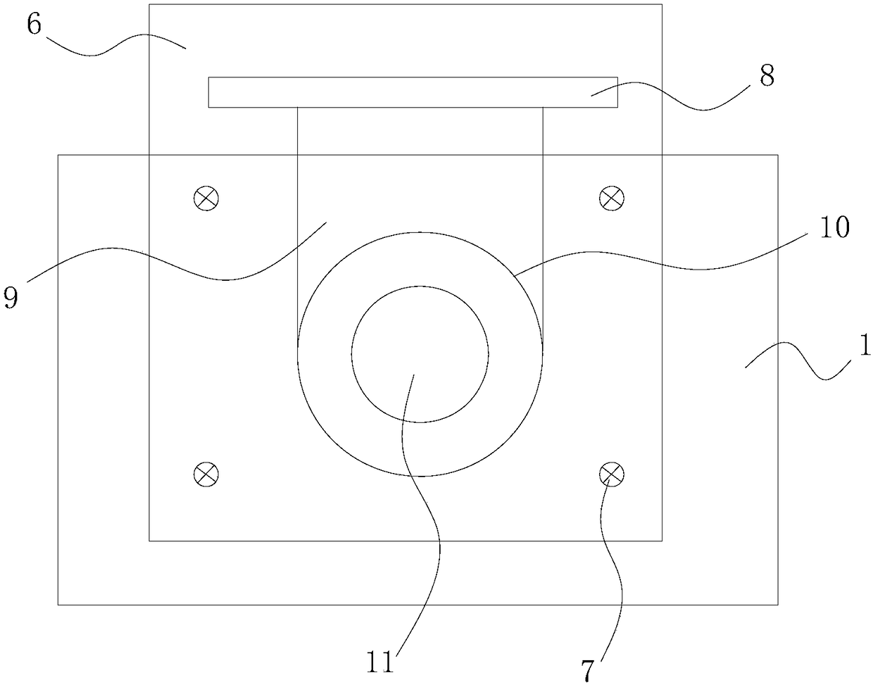
[0026] The preferred embodiment discloses a semiconductor wafer electrodeposition method. In the electrodeposition method, the anode only conducts electrodeposition on the middle of the semiconductor wafer to be electrodeposited, so as to avoid the concentration of electric field lines at the edge of the semiconductor wafer to be electrodeposited and produce edge effects. The specific area, shape, and area percentage of the "middle part" on the entire semiconductor wafer to be electrodeposited are not limited, and can be determined according to specific needs, so as to avoid electric field lines on the semiconductor wafer to be electrodeposited. The purpose of concentrating at the edges and creating edge effects is sufficient.

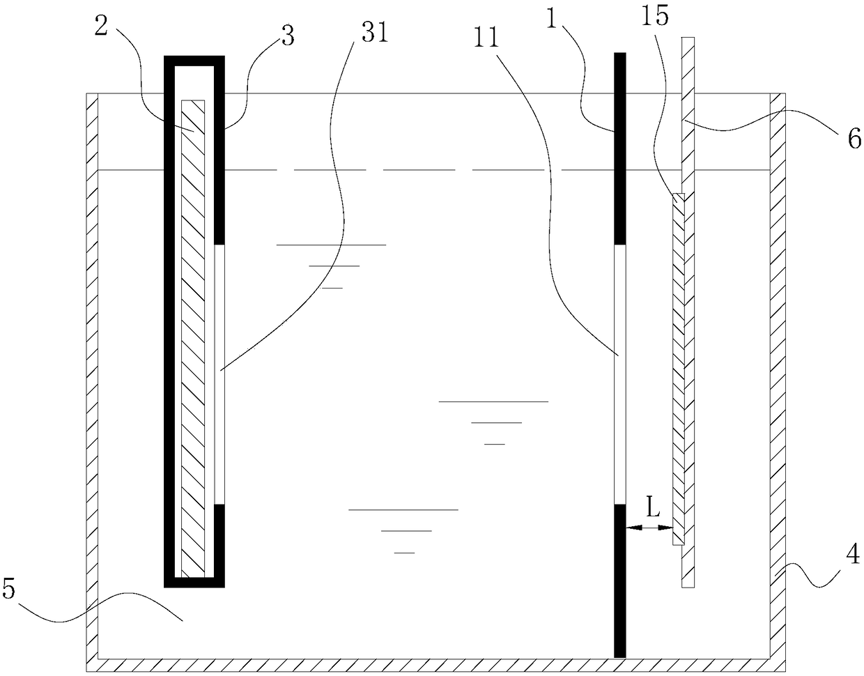
[0027] like figure 1 and figure 2 A...


PUM


Abstract

The invention discloses a semiconductor wafer electro-deposition method and a semiconductor wafer electro-deposition device and belongs to the field of semiconductor wafer electro-deposition. The semiconductor wafer electro-deposition method and the semiconductor wafer electro-deposition device are designed for solving the problems of poor uniformity of electro-deposition layers in the prior art.According to the semiconductor wafer electro-deposition method, an anode is used for conducting electro-deposition only on the middle portion of a semiconductor wafer to be electro-deposited so as toprevent the fringe effect from being generated when electric field lines are centralized at the edge of the semiconductor wafer to be electro-deposited. The semiconductor wafer electro-deposition device comprises a clamp, a baffle and the anode. An interval is reserved between the semiconductor wafer to be electro-deposited and the baffle. The baffle is provided with a baffle through hole. The baffle through hole corresponds to the semiconductor wafer to be electro-deposited, and the area of the baffle through hole is smaller than that of the semiconductor wafer to be electro-deposited. Through the semiconductor wafer electro-deposition method and the semiconductor wafer electro-deposition device, the electro-deposition fringe effect is eliminated, and the electro-deposition uniformity isimproved.

Description

technical field [0001] The invention relates to the field of semiconductor wafer electrodeposition, in particular to a semiconductor wafer electrodeposition method and a semiconductor wafer electrodeposition device for realizing the electrodeposition method. Background technique [0002] Depositing a metal layer is usually an indispensable step in the wafer, and the uniformity of the thickness of the electrodeposited metal on the surface of the wafer is an important indicator that affects the performance and yield of chips made on the wafer. [0003] In order to improve the uniformity of electrodeposited metal thickness, the existing main method is to reduce the current density during electrodeposition. This method improves the uniformity of the deposited layer by reducing the electrodeposition rate and increasing the electrodeposition time, but since each deposition solution can only work at a certain current density, simply reducing the electrodeposition rate will lead to ...

Claims


Application Information

Patent Timeline
IPC IPC(8): C25D7/12C25D17/00C25D17/06
Inventor 金鑫
Owner DYNAX SEMICON
Why Eureka
Try Eureka