Optimization method of bending of wafer

An optimization method and bending technology, applied to electrical components, circuits, semiconductor devices, etc., can solve problems such as wafer quality degradation, wafer surface depressions or protrusions, etc., and achieve the effect of improving quality

Inactive Publication Date: 2018-06-01
HUAIAN IMAGING DEVICE MFGR CORP
View PDF3 Cites 10 Cited by
  • Summary
  • Abstract
  • Description
  • Claims
  • Application Information

AI Technical Summary

Problems solved by technology

[0002] In the existing semiconductor device manufacturing technology, it is easy to form an overall depression or protrusion on the surface of the wafer, which leads to the deterioration of the quality of the wafer in subsequent bonding (Bonding) and other process steps.

Method used


Image

  • Optimization method of bending of wafer
  • Optimization method of bending of wafer
  • Optimization method of bending of wafer

Examples


Embodiment Construction

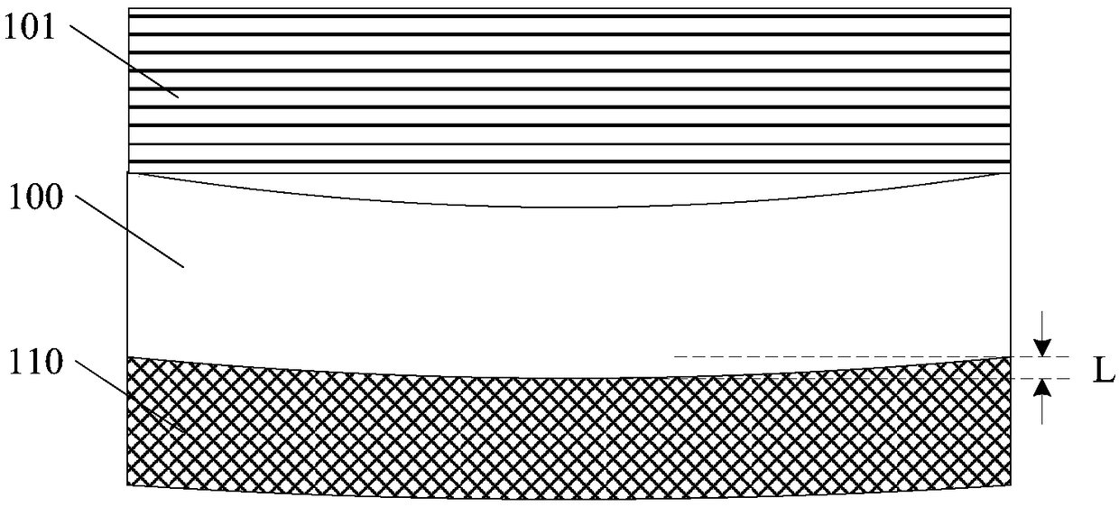
[0027] In the existing semiconductor device manufacturing technology, it is easy to appear the phenomenon that the surface of the wafer forms an overall depression or protrusion, which leads to the deterioration of the quality of the wafer in subsequent process steps such as bonding.

[0028] figure 1 It is a schematic cross-sectional structure diagram of a curved wafer in the prior art. Such as figure 1 As shown, the overall dishing of the wafer 100 occurs during the process, resulting in a decrease in quality in subsequent process steps such as bonding. Specifically, for example, when the device formed on the wafer 100 is a backside illumination-CMOS Image Sensors (BSI-CIS), the wafer 100 and the carrier wafer (Carrier Wafer) 101 need to be bonded , for other semiconductor devices, it may also be necessary to bond the wafer 100 to another device wafer (Device Wafer).

[0029] Wherein, the wafer 100 can be, for example, a device wafer, so that various semiconductor devices...


PUM


Abstract

Provided is an optimization method of the bending of a wafer. The method includes following steps: the wafer is provided, a crystal surface SiN is formed on the front surface of the wafer, a crystal back SiN is formed at the backside of the wafer, the crystal surface SiN and the crystal back SiN are formed in the same furnace tube process, and the front surface of the wafer is processed to form anacid-corrosion-resistant protective layer on the front surface; and under the protection of the protective layer, at least a part of the crystal back SiN is removed by employing acid. According to the scheme of the method, the bending of the wafer can be adjusted, and the quality of process steps including subsequent bonding can be improved through reduction of adjustment of the bending of the wafer.

Description

technical field [0001] The invention relates to the field of semiconductor manufacturing, in particular to a method for optimizing wafer curvature. Background technique [0002] In the existing manufacturing technology of semiconductor devices, it is easy to appear the phenomenon of overall depression or protrusion on the surface of the wafer, which leads to the deterioration of the quality of the wafer in subsequent process steps such as bonding (Bonding). [0003] Bending of Wafer (BOW) is usually used to evaluate the degree of concave or convex of a wafer, and the BOW of wafer is used to indicate the vertical distance between the highest point and the lowest point of the wafer surface. [0004] There is an urgent need for a method for optimizing the curvature of the wafer to adjust the curvature of the wafer to improve the quality of subsequent bonding and other process steps. Contents of the invention [0005] The technical problem solved by the present invention is t...

Claims


Application Information

Patent Timeline
IPC IPC(8): H01L29/06H01L21/02
CPCH01L21/02008H01L21/02035H01L29/06
Inventor 杨鸣鹤陈世杰黄晓橹
Owner HUAIAN IMAGING DEVICE MFGR CORP
Why Eureka
Try Eureka