


Quick Research
Generate reliable direction feasibility study reports for your R&D in just a few steps.

Technical Q&A
Discover and master advanced knowledge NOW. Basics, ideas, possibilities, all at once.

Find Solutions
As an expert in R&D theories, this can generate solutions to your technical problems instantly.

Evaluate Feasibility
Analyze your overall solution with one click, know your potential R&D risks in advance.

Monitor Landscape
Get weekly tech updates, stay abreast of the latest tech innovations and key insights.
Programming method and device of memory unit
A technology of storage unit and programming method, which is applied in the field of storage, can solve problems such as slow programming speed, achieve the effect of reducing influence and improving programming performance
- Summary
- Abstract
- Description
- Claims
- Application Information
AI Technical Summary
Problems solved by technology
Method used
Image


Examples
Embodiment 1
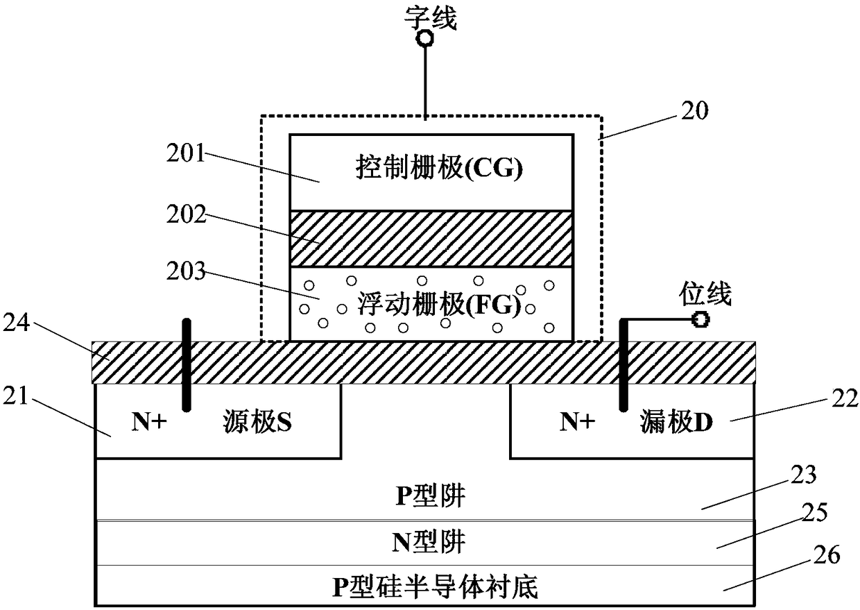
[0040] figure 2 It is a schematic flow chart of a method for programming a memory cell provided by Embodiment 1 of the present invention. This embodiment is applicable to the case of performing programming operations on memory cells at different temperatures. see figure 2 The programming method of the storage unit provided in this embodiment specifically includes the following steps:
[0041] 110. Receive a programming instruction.
[0042] By writing program codes, the flash memory can be controlled to perform three main operations, which are read operation, write operation (ie, programming operation) and erasing operation, wherein the programming operation is specifically to complete the operation of writing 0 to the storage unit. The basic principle of programming a memory cell is to apply corresponding programming voltages to the gate and drain of the memory cell respectively. After applying the programming voltage, a current will flow from the drain to the source, and...
Embodiment 2
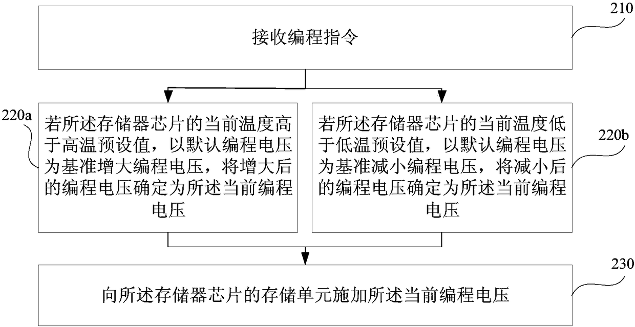
[0054] image 3 It is a schematic flow chart of a programming method for a storage unit provided in Embodiment 2 of the present invention. This embodiment is further optimized on the basis of Embodiment 1, especially applicable to the situation where the programming speed changes due to the temperature change of the memory chip. The advantage is that when the temperature of the memory chip is higher than the high-temperature preset value or lower than the low-temperature preset value, the programming voltage matching the temperature is determined to ensure the programming speed at high temperature and improve the excessive programming at low temperature. problems and improve programming performance. For details, please refer to image 3 , the method specifically includes the following steps:
[0055] 210. Receive a programming instruction.
[0056] 220a. If the current temperature of the memory chip is higher than the high temperature preset value, increase the programming ...
Embodiment 3
[0065] Figure 4 It is a schematic structural diagram of a memory cell programming device provided in Embodiment 3 of the present invention, and the device specifically includes:
[0066] receiving module 410, determining module 420 and applying module 430;
[0067] Among them, the receiving module 410 is used to receive programming instructions; the determining module 420 is used to determine the current programming voltage according to the current temperature of the memory chip; the applying module 430 is used to apply the current programming voltage to the memory cells of the memory chip.
[0068] Further, the device may further include a detection module, configured to detect the current temperature of the memory chip through a temperature sensor before determining the current programming voltage according to the current temperature of the memory chip.
[0069] Further, the determining module 420 may include:
[0070] An increasing unit, configured to increase the progra...
PUM
 Abstract
Description
Claims
Application Information
 - R&D Engineer
- R&D Manager
- IP Professional
- Industry Leading Data Capabilities
- Powerful AI technology
- Patent DNA Extraction
Browse by: Latest US Patents, China's latest patents, Technical Efficacy Thesaurus, Application Domain, Technology Topic, Popular Technical Reports.
© 2024 PatSnap. All rights reserved.Legal|Privacy policy|Modern Slavery Act Transparency Statement|Sitemap|About US| Contact US: help@patsnap.com