LED wafer cutting device

A technology for cutting devices and wafers, which is applied to fine working devices, stone processing equipment, manufacturing tools, etc. It can solve problems such as complicated procedures, low work efficiency, and low safety performance, and achieve simple operation, reduced costs, and improved work efficiency. efficiency effect

Inactive Publication Date: 2018-05-29
湖南华特光电科技有限公司
View PDF6 Cites 2 Cited by
  • Summary
  • Abstract
  • Description
  • Claims
  • Application Information

AI Technical Summary

Problems solved by technology

[0012] Aiming at the deficiencies of the prior art, the present invention provides an LED wafer cutting device, which solves the problems of the existing LED wafer cutting device, such as low safety performance, troublesome and complicated process, and low work efficiency

Method used


Image

  • LED wafer cutting device
  • LED wafer cutting device

Examples


Embodiment Construction

[0027] The technical solutions in the embodiments of the present invention will be clearly and completely described below with reference to the accompanying drawings in the embodiments of the present invention. Obviously, the described embodiments are only a part of the embodiments of the present invention, but not all of the embodiments. Based on the embodiments of the present invention, all other embodiments obtained by those of ordinary skill in the art without creative efforts shall fall within the protection scope of the present invention.

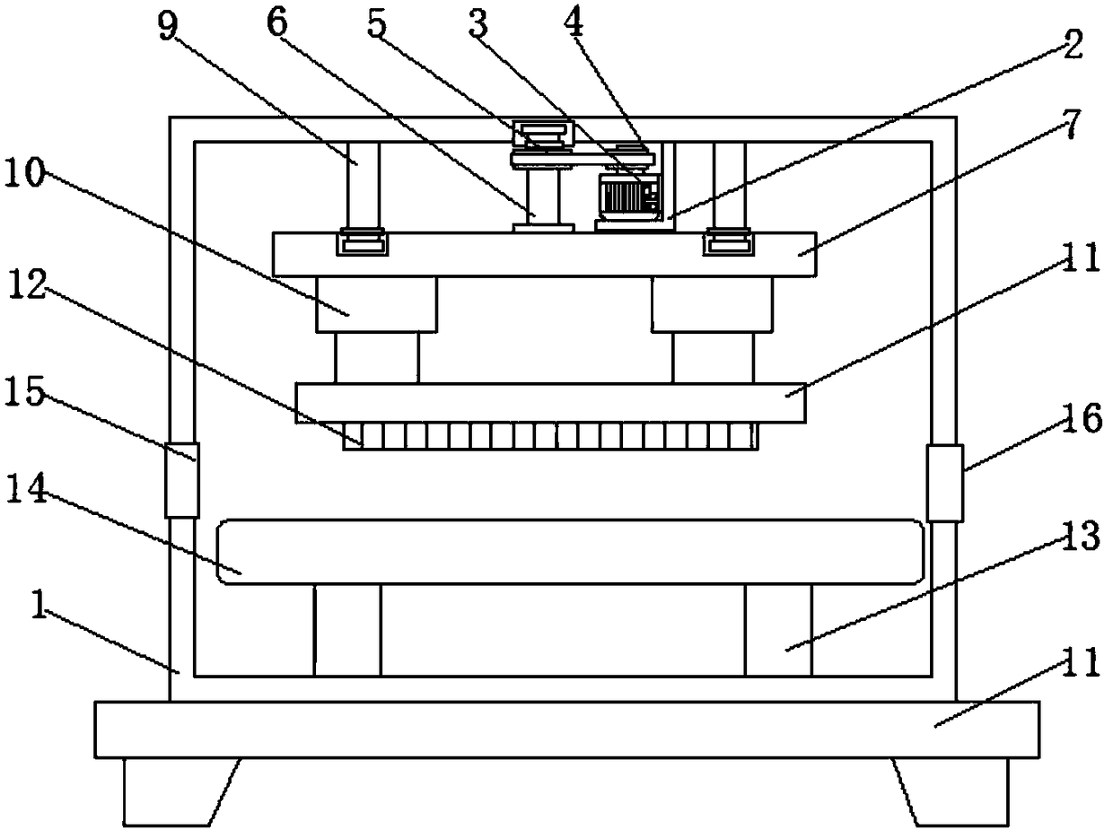
[0028] see Figure 1-2 , the present invention provides a technical solution: an LED chip cutting device, comprising a box body 1, an L-shaped connecting plate 2 is fixedly connected to the top of the inner wall of the box body 1, and a motor 3 is fixedly connected to the top of the L-shaped connecting plate 2, The output shaft of the motor 3 is fixedly connected with a first pulley 4, and the surface of the first pulley 4 is connecte...


PUM


Abstract

The invention discloses an LED wafer cutting device. The LED wafer cutting device comprises a box c, the top of the inner wall of the box body is fixedly connected with an L-shaped connecting plate, and the top of the L-shaped connecting plate is fixedly connected with a motor; a first belt pulley is fixedly connected to an output shaft of the motor, and a second belt pulley is connected to the surface of the first belt pulley through a belt in a transmission mode; a first rotating shaft penetrates through the middle of the second belt pulley, and the top end of the first rotating shaft is rotatably connected with the top of the inner wall of the box body; the bottom end of the first rotating shaft is fixedly connected with a connecting plate, and both sides of the bottom of the connectingplate are fixedly connected with telescopic cylinders; and a cross bar is fixedly connected to the bottom parts of the telescopic cylinders, and a cutting blade is fixedly connected to the bottom endof the cross bar. The invention relates to the technical field of wafer cutting equipment. The LED wafer cutting device solves the problems of low safety performance, complicated procedures and low work efficiency of an existing LED wafer cutting device.

Description

technical field [0001] The invention belongs to the technical field of wafer cutting equipment, and in particular relates to an LED wafer cutting device. Background technique [0002] LED is the abbreviation of "Light Emitting Diode", which is translated into "Light Emitting Diode" in Chinese. It is a semiconductor device that can convert electrical energy into light energy. The chip is the core part of the LED, and chips of different materials can emit light of different colors such as red, orange, yellow, green, blue, and purple. The production process of LED can be divided into substrate preparation, epitaxial wafer and chip production, packaging and application, and the application includes signal and indication, backlight, lighting, display screen, etc. [0003] my country's LED application is the fastest growing link in the LED industry chain, with an overall growth rate of nearly 38% in 2014. Among them, the growth rate of the general lighting market is about 69%, a...

Claims


Application Information

Patent Timeline
Patent Type & Authority Applications(China)
IPC IPC(8): B28D5/04B28D5/00
CPCB28D5/042B28D5/0082
Inventor 曹毅曹财铭
Owner 湖南华特光电科技有限公司
Why Eureka
Try Eureka