LED packaging structure

A technology of LED packaging and heat dissipation substrate, applied in semiconductor devices, electrical components, circuits, etc., can solve the problems of insufficient concentration of light source lighting, affecting light transmission efficiency, reducing light intensity, etc., to suppress total reflection effect, reduce costs, The effect of increasing the cooling effect

Active Publication Date: 2018-05-08
广东安林电子科技股份有限公司
View PDF4 Cites 0 Cited by
  • Summary
  • Abstract
  • Description
  • Claims
  • Application Information

AI Technical Summary

Problems solved by technology

First of all, the light emitted by the LED light source is generally distributed in a divergent manner, that is, the Lambertian distribution, which leads to insufficient illumination brightness of the light source, and generally requires secondary shaping through an external lens to meet the lighting needs of specific occasions, thus increasing production costs; secondly , only a part of the energy in the LED input power is converted into light energy, and the rest of the energy is converted into heat energy. Therefore, for LED chips, especially LED chips with high power density, how to control their energy is a key issue for LED manufacturers and lamps. Finally, because high-power LEDs are used in lighting and other occasions, cost control is very important, and the structural size of the external heat sink of high-power LED lamps is not allowed to be too large, and it is impossible to allow active cooling by adding electric fans, etc. The safe junction temperature of the LED chip should be within 110°C. If the junction temperature is too high, it will lead to a series of problems such as reduced light intensity, spectral shift, increased color temperature, increased thermal stress, and accelerated aging of the chip, which greatly reduces the performance of the LED chip. At the same time, it can also lead to accelerated aging of the encapsulation glue filled on the chip, affecting its light transmission efficiency

Method used


Image

  • LED packaging structure
  • LED packaging structure
  • LED packaging structure

Examples


Embodiment 1

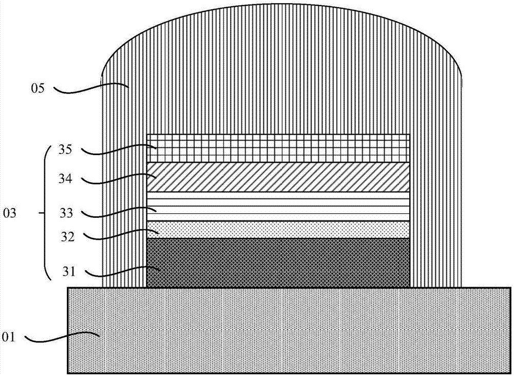
[0043] See figure 1 , figure 1 It is a schematic diagram of an LED package structure provided by an embodiment of the present invention. The structure includes:

[0044] heat dissipation substrate 01;

[0045] The ultraviolet lamp wick 03 is arranged on the upper surface of the heat dissipation substrate;

[0046] The silica gel layer 05 is disposed on the heat dissipation substrate and the upper surface of the ultraviolet lamp wick.

[0047] Wherein, the material of the heat dissipation substrate 01 is copper.

[0048] Further, the outer side of the heat dissipation substrate 01 is provided with circular grooves along the width direction and parallel to the plane of the heat dissipation substrate; wherein, the diameter of the circular grooves is 0.3-2 mm, and the spacing between the circular grooves is 0.5-10 mm.

[0049] Wherein, the ultraviolet lamp wick 03 includes an n-AlGaN layer 32, an MQW layer 33, a p-AlGaN layer 34, and a p-GaN layer 35 sequentially disposed on ...

Embodiment 2

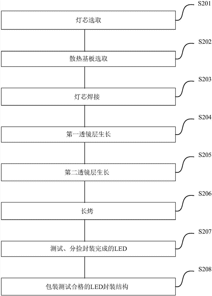
[0066] See figure 2 , figure 2 This is a flow chart of a method for packaging a double-lens layer LED according to an embodiment of the present invention. On the basis of the above embodiments, this embodiment will introduce the process flow of the double-lens layer LED package proposed by the present invention in more detail. The method includes:

[0067] S201, wick selection

[0068] The UV wick was chosen as the wick of the LED.

[0069] S202, heat dissipation substrate selection

[0070] Only a part of the LED input power is converted into light energy, and the rest is converted into heat energy. Therefore, for LED chips, especially LED chips with high power density, how to control their thermal energy is an important problem that LED manufacturing and lamps should focus on. The heat of high-power diodes, high-power triodes, IGBTs, and MOSFETs can be dissipated through an external radiator with almost unlimited size installed on the chassis of the instrument, or a ...

Embodiment 3

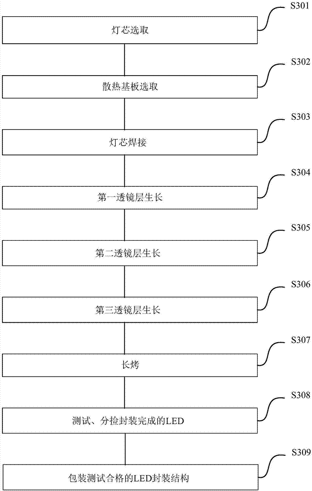
[0115] See image 3 , image 3 A flow chart of a three-layer lens layer LED packaging method provided in an embodiment of the present invention. On the basis of the above embodiments, this embodiment will introduce the process flow of the three-layer lens layer LED packaging proposed by the present invention in more detail. include:

[0116] S301, wick selection

[0117] The UV wick was chosen as the wick of the LED.

[0118] S302, heat dissipation substrate selection

[0119] S3021, bracket / cooling substrate preparation

[0120] Metal copper is selected as the material of the heat dissipation substrate, and the thickness of the heat dissipation substrate is 0.5-10 mm. The outer side of the heat dissipation substrate is provided with a circular groove along the width direction and parallel to the plane of the heat dissipation substrate; wherein the diameter of the circular groove is 0.3-2 mm, and the distance between the circular grooves is 0.5-10 mm. The circular groov...


PUM


Abstract

The invention relates to an LED packaging structure, which comprises a heat dissipation substrate 01, an ultraviolet lamp core 03 and a silica gel layer 05, wherein the ultraviolet lamp core 03 is arranged on the upper surface of the heat dissipation substrate; and the silica gel layer 05 is arranged on the heat dissipation substrate and the upper surface of the ultraviolet lamp core. According tothe LED packaging structure provided by the invention, the refractive indexes are sequentially increased through multiple lens layers, so that the light transmittance of the LED lamp core can be improved, and more light emitted from the LED lamp core can shine out through a packaging material.

Description

technical field [0001] The present invention relates to the technical field of packaging, in particular to an LED packaging structure. Background technique [0002] LED has the characteristics of long life, high luminous efficiency, good color rendering, safe and reliable, rich color and easy maintenance. Under the background of increasingly serious environmental pollution, climate warming and energy shortage, semiconductor lighting technology based on high-power LED has been recognized as one of the most promising high-tech fields in the 21st century. This is a great leap in the history of human lighting since gas lighting, incandescent lamps and fluorescent lamps, and has rapidly improved the lighting quality of human life. [0003] In recent years, LEDs mostly use the method of ultraviolet lamp core and RGB three primary colors to generate white light to realize illumination. This method has the following problems. First of all, the light emitted by the LED light source...

Claims


Application Information

Patent Timeline
Patent Type & Authority Applications(China)
IPC IPC(8): H01L33/50H01L33/56H01L33/64H01L33/58
CPCH01L33/504H01L33/507H01L33/56H01L33/58H01L33/642H01L33/648
Inventor 尹晓雪
Owner 广东安林电子科技股份有限公司
Why Eureka
Try Eureka