Lithium niobate film electro-optical modulator with high modulation efficiency
An electro-optic modulator, lithium niobate technology, applied in the direction of instruments, optics, nonlinear optics, etc., to achieve the effect of reducing half-wave voltage and short electrode spacing
- Summary
- Abstract
- Description
- Claims
- Application Information
AI Technical Summary
Problems solved by technology
Method used
Image
Examples
Embodiment 1
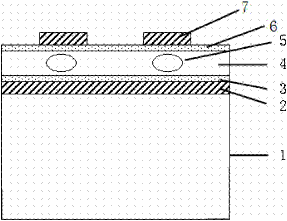
[0021] Such as figure 1 As shown, this embodiment includes a base material 1, a lower electrode 2, a lower buffer layer 3, a lithium niobate thin film 4, an optical waveguide 5, an upper buffer layer 6, and an upper electrode 7. The upper electrode 7 is a signal level, including positive electrode and negative electrode, the positive electrode and the negative electrode are respectively located above the optical waveguides 5 on the left and right sides, the lower electrode is the ground electrode, and the lithium niobate thin film 4 is niobium with a single crystal structure and a thickness of 0.1 μm to 10 μm Lithium oxide film material. The base material 1 adopts a z-cut lithium niobate bulk crystal material with a thickness of 0.1mm to 2mm; the lower electrode 2 adopts a metal film such as gold or aluminum with a thickness of 0.1um to 30um; the lower buffer layer 3 and the upper The buffer layer 2 adopts an oxide film such as silicon dioxide or aluminum oxide with a thickne...
Embodiment 2
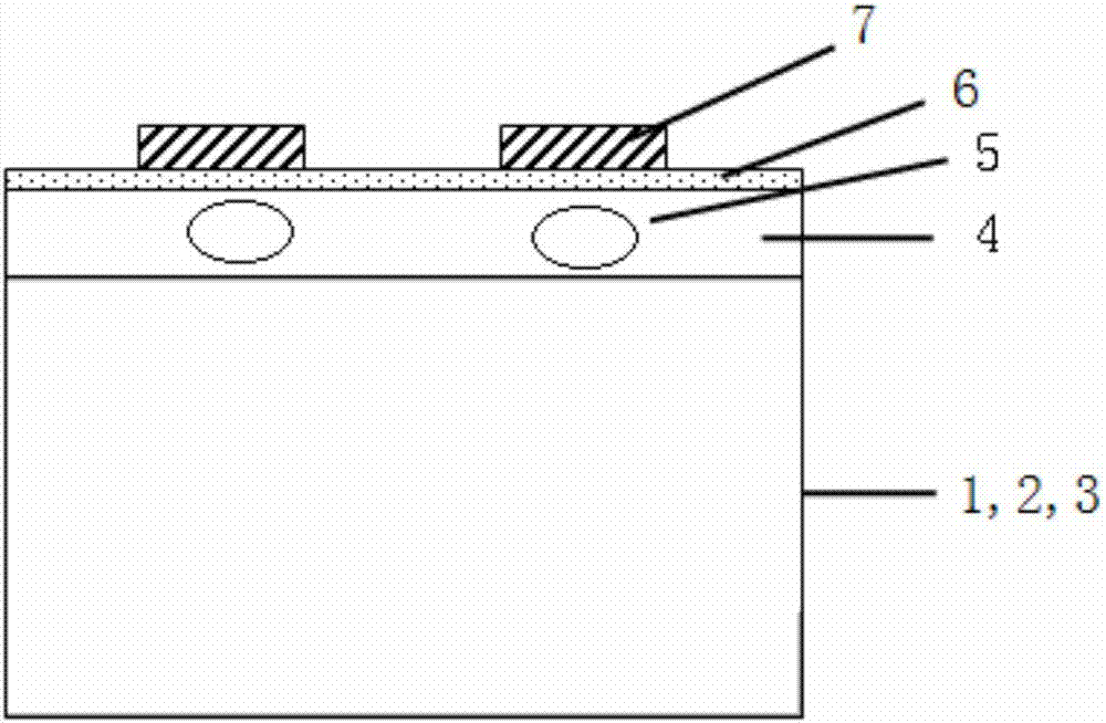
[0023] Such as figure 2 As shown, the difference between this embodiment and Embodiment 1 is that the low-resistance silicon base material replaces the lithium niobate bulk crystal base material 1, the lower electrode 2, and the lower buffer layer 3 in the above-mentioned scheme. The characteristics play the role of the lower electrode 2, and the silicon substrate and the metal shell are bonded through the conductive glue to make the low-resistance silicon substrate a ground electrode; the upper buffer layer 6 is made of silicon dioxide or oxide with a thickness of 0.1um to 5um. An oxide film such as aluminum; the upper electrode 7 adopts a metal film such as gold or aluminum with a thickness of 0.1um to 30um.
Embodiment 3
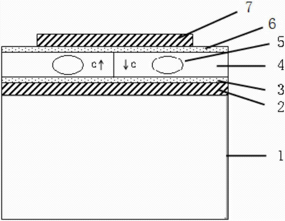
[0025] This embodiment provides a new lithium niobate thin film (4) structure on the basis of embodiment 1 or embodiment 2, and the rest of the scheme is consistent with embodiment 1 or embodiment 2. The lithium niobate film (4) is composed of a left half film part and a right half film part, wherein the left half film part has a +c polarization direction or a -c polarization direction, and correspondingly, the right half film Part has -c polarization direction or +c polarization direction, that is, when the left half film part has +c polarization direction, the right half film part has -c polarization direction, when the left half film part has -c polarization direction, the right half film part has +c polarization direction. Such as image 3 Shown is the illustration of the improvement carried out on the basis of embodiment 1.
PUM
| Property | Measurement | Unit |
|---|---|---|
| thickness | aaaaa | aaaaa |
| thickness | aaaaa | aaaaa |
Abstract
Description
Claims
Application Information
 - R&D Engineer
- R&D Manager
- IP Professional
- Industry Leading Data Capabilities
- Powerful AI technology
- Patent DNA Extraction
Browse by: Latest US Patents, China's latest patents, Technical Efficacy Thesaurus, Application Domain, Technology Topic, Popular Technical Reports.
© 2024 PatSnap. All rights reserved.Legal|Privacy policy|Modern Slavery Act Transparency Statement|Sitemap|About US| Contact US: help@patsnap.com


