Circuit and nand flash for reducing programming setup time of nand flash

A technology of establishing time and circuits, which is applied in the field of NAND flash memory, can solve the problems of long voltage establishing time and restricting the programming speed of NAND FLASH, and achieve the effect of reducing voltage establishing time, increasing programming speed and reducing equivalent capacitance

Active Publication Date: 2020-09-18
GIGADEVICE SEMICON (BEIJING) INC
View PDF11 Cites 0 Cited by
  • Summary
  • Abstract
  • Description
  • Claims
  • Application Information

AI Technical Summary

Problems solved by technology

[0003] In view of the above problems, the purpose of the embodiments of the present invention is to provide a circuit that reduces the programming setup time of NAND flash memory and a kind of NAND flash memory, to solve the problem that the voltage setup time of selected WL is long and restricts the programming speed of NAND FLASH

Method used


Image

  • Circuit and nand flash for reducing programming setup time of nand flash
  • Circuit and nand flash for reducing programming setup time of nand flash
  • Circuit and nand flash for reducing programming setup time of nand flash

Examples


Embodiment Construction

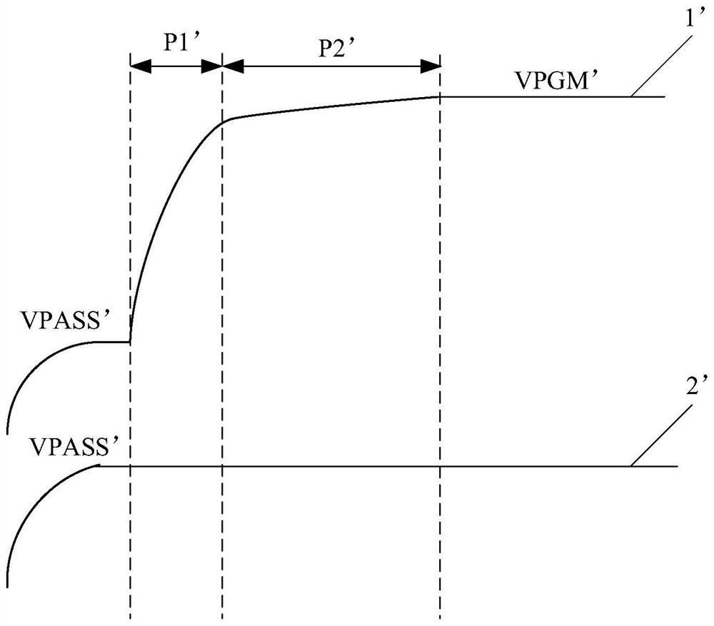
[0021] In order to make the above objects, features and advantages of the present invention more comprehensible, the present invention will be further described in detail below in conjunction with the accompanying drawings and specific embodiments.

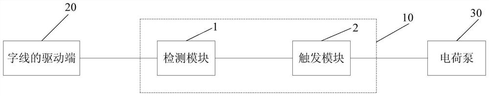
[0022] refer to figure 2 , shows a structural block diagram of an embodiment of a circuit 10 for reducing the programming setup time of NAND flash memory of the present invention, which may specifically include the following modules: a detection module 1, which is connected to the drive terminal 20 of a word line in the NAND flash memory , when the word line is selected, the detection module 1 detects the drive terminal voltage of the word line in real time, and generates a detection voltage according to the drive terminal voltage of the word line; the trigger module 2, the input terminal of the trigger module 2 is connected with the output terminal of the detection module 1, The output terminal of the trigger module 2 is connect...


PUM


Abstract

The embodiments of the present invention provide a circuit for reducing the programming establishment time of a NAND flash memory, and a NAND flash memory. The circuit comprises: a detection module connected to the drive terminal of a word line in a NAND flash memory, wherein the detection module detects the voltage of the drive terminal of the word line when the word line is selected, and generates a detection voltage according to the voltage of the drive terminal of the word line; a trigger module, wherein the input terminal of the trigger module is connected to the output terminal of the detection module, the output terminal of the trigger module is connected to at least one charge pump corresponding to the unselected work line adjacent to the word line, the trigger module triggers at least one charge pump when the detection voltage is higher than a preset reference voltage so as to make the charge pump output a first voltage to the unselected work line adjacent to the word line, and the first voltage is higher than 0 V and is less than the programming voltage of the word line. With the embodiments of the present invention, the voltage establishment time of the selected word line can be effectively reduced so as to improve the programming speed of the NAND flash memory.

Description

technical field [0001] The invention relates to the field of memory technology, in particular to a circuit for reducing the programming setup time of a NAND flash memory and a NAND flash memory. Background technique [0002] In the prior art, when NAND FLASH (flash memory) is programmed, a voltage VPGM' of about 20V is applied to the selected WL (word line) through a charge pump (Pump), and a voltage VPASS' of about 10V is applied to the unselected WL. like figure 1 As shown, in the P1' phase, the voltage on the selected WL is low, and the charge pump can provide a strong current to charge the selected WL, so the voltage on the selected WL rises rapidly, figure 1 Among them, 1' is the voltage establishment waveform of the selected word line, and 2' is the voltage establishment waveform of the unselected word line. But when the P2' stage is reached, since the voltage on the selected WL is close to the final value VPGM', the current provided by the charge pump to the selecte...

Claims


Application Information

Patent Timeline
Patent Type & Authority Patents(China)
IPC IPC(8): G11C16/10G11C16/34
CPCG11C16/10G11C16/34
Inventor 朱长峰李琪
Owner GIGADEVICE SEMICON (BEIJING) INC
Why Eureka
Try Eureka