Eureka AIR delivers breakthrough ideas for toughest innovation challenges, trusted by R&D personnel around the world.

Protection structure and method for electromagnetic attack protection of chip

A technology for protecting structures and electromagnetic attacks, applied in internal/peripheral computer component protection, measuring electricity, measuring electrical variables, etc., can solve problems such as chip internal state or internal password operation errors

Inactive Publication Date: 2018-04-20
BEIJING CEC HUADA ELECTRONIC DESIGN CO LTD
View PDF13 Cites 5 Cited by
  • Summary
  • Abstract
  • Description
  • Claims
  • Application Information

AI Technical Summary

Problems solved by technology

[0003] Fault injection attacks cause errors in the internal state of the chip or internal cryptographic operations by injecting interference signals into the security chip at a specific moment

Method used


Image

  • Protection structure and method for electromagnetic attack protection of chip
  • Protection structure and method for electromagnetic attack protection of chip
  • Protection structure and method for electromagnetic attack protection of chip

Examples


Embodiment Construction

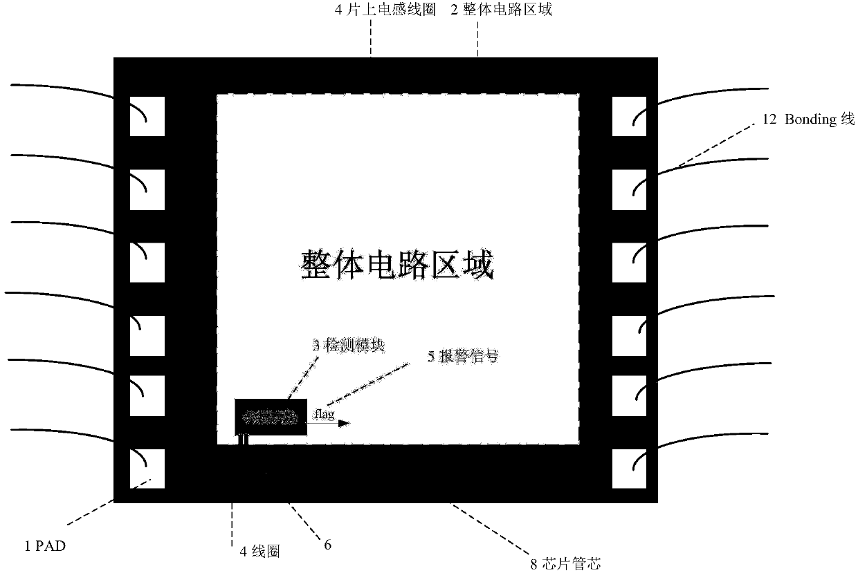
[0023] Such as figure 1 As shown in , it includes the internal structure of the chip to realize the electromagnetic attack protection of the whole chip (2). It is mainly composed of an on-chip inductance coil (4), a signal connection line (6), a detection module (3), and an output alarm signal (5).

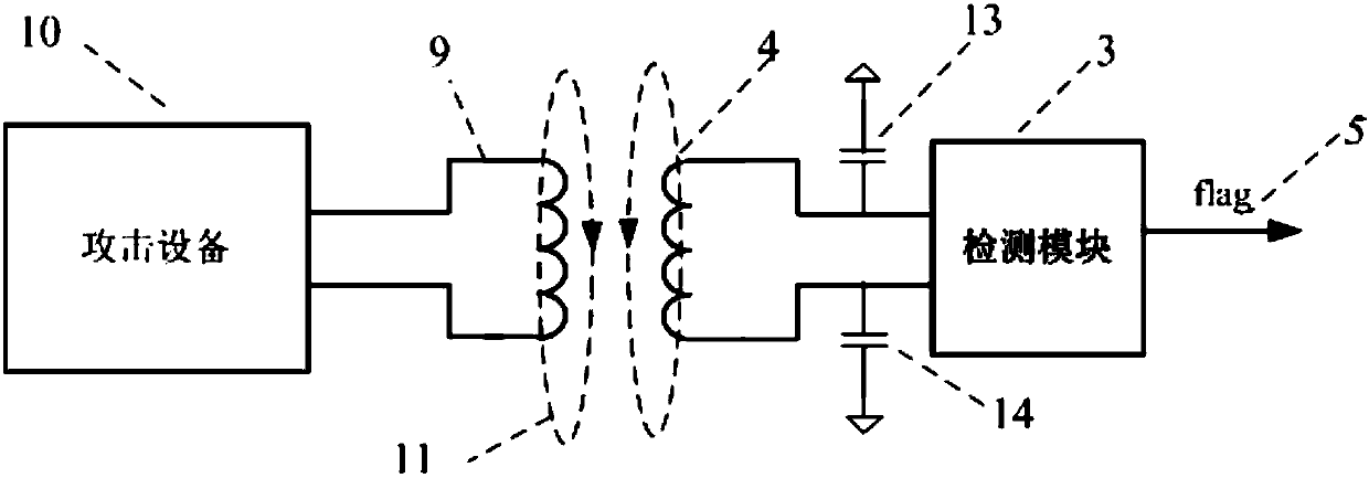
[0024] Such as figure 2 As shown, it includes the structure inside the chip to realize the electromagnetic attack protection of the chip part (7). It is mainly composed of an on-chip inductance coil (4), a signal connection line (6), a detection module (3), and an output alarm signal (5).

[0025] The specific protection methods are implemented as follows:

[0026] 1) When the chip is attacked under the attacking device (10), it emits an electromagnetic field (11) with considerable strength, the coupling coefficient is adjusted by adjusting the capacitors (13), (14), and the electromagnetic field signal is sampled through the on-chip inductance coil (4) .

[0027] 2) The ele...


PUM


Abstract

The invention proposes a protection structure and method for the electromagnetic attack protection of a chip, and the structure and method achieve the protection of the whole chip or a part of the chip against the electromagnetic fault injection attack under the condition that the performances of the chip are not affected. The method is low in cost, is reliable in performance, and is wide in application range. The method employs an on-chip inductor to surround a to-be-protected overall circuit or circuit part. When there is an electromagnetic injection attack, the on-chip inductor carries outthe sampling of an electromagnetic signal injected during an inductor fault, a sampled voltage or current signal is converted into an alarm signal for output through a detection module, thereby achieving a purpose of fault injection protection.

Description

technical field [0001] The invention relates to a protection method suitable for chip electromagnetic attack protection. When a chip is attacked by a strong electromagnetic field injection, it is likely to generate fault or error information that can be used by the attacker. With the reduction of the process size, the attack More and more effective, becoming a common method of fault attack. The invention proposes an electromagnetic attack protection method implemented inside the chip, which is simple, reliable, easy to implement, and low in cost; in addition, by adjusting the position and shape of the on-chip inductance, the whole chip protection and local area protection can be flexibly realized. Background technique [0002] In recent years, there have been more and more attack methods targeting security chips that provide cryptographic security services. These attack methods are commonly used in invasive, non-invasive and semi-invasive methods. Intrusive attack methods ...

Claims


Application Information

Patent Timeline
IPC IPC(8): G01R31/00G01R19/165G06F21/76
CPCG01R19/16571G01R19/16576G01R31/001G06F21/76
Inventor 陈永强陈波涛
Owner BEIJING CEC HUADA ELECTRONIC DESIGN CO LTD
Why Eureka
Eureka Blog
Learn More