Trench epitaxy filling method

A filling method and trench technology, applied in electrical components, semiconductor/solid-state device manufacturing, circuits, etc., can solve problems affecting device performance and other issues, and achieve the effect of reducing the amount of lateral etching

Active Publication Date: 2018-04-17
SHANGHAI HUAHONG GRACE SEMICON MFG CORP
View PDF5 Cites 2 Cited by
  • Summary
  • Abstract
  • Description
  • Claims
  • Application Information

AI Technical Summary

Problems solved by technology

Since the epitaxial growth process is selected to grow on the surface of the epitaxial layer, and not to grow on the surface of the oxide layer, during the epitaxial growth process, the P-type epitaxial layer 106 will be formed on the side surface and bottom surface of the trench 201 and the undeveloped area outside the trench 201 at the same time. The surface of the N-type epitaxial layer 102 covered by the oxide layer 103 grows simultaneously, and the thickness of the P-type epitaxial layer 106 formed on the surface of the N-type epitaxial layer 102 not covered by the oxide layer 103 outside the trench 201 is greater than the thickness of the oxide layer 103. It will extend to the surface of the oxide layer 103 and grow laterally at the same time, finally making the P-type epitaxial layer 106 in the adjacent trenches 201 easily extend to each other on the surface of the oxide layer 103 between the trenches 201 to contact and merge to form an integral structure , the P-type epitaxial layer 106 formed on the oxide layer 103 and laterally contacting and merging with each other tends to generate stress and form dislocations (dislocation), which will eventually affect the performance of the device

Method used


Image

  • Trench epitaxy filling method
  • Trench epitaxy filling method
  • Trench epitaxy filling method

Examples


Embodiment Construction

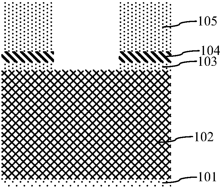
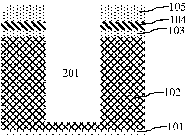
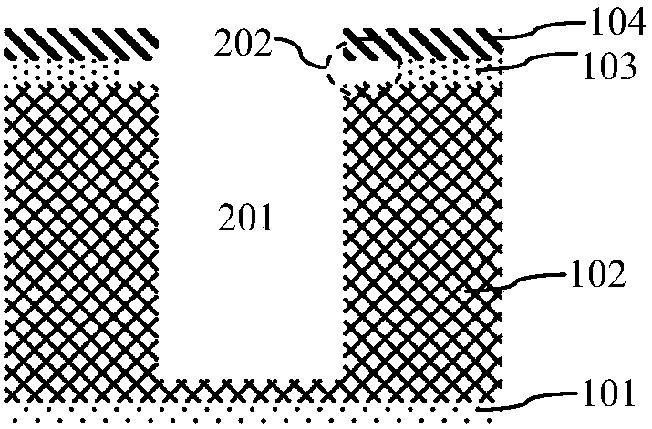
[0041] Such as figure 2 Shown is the flow chart of the filling method of trench epitaxy in the embodiment of the present invention; as Figure 3A to Figure 3I As shown, it is a schematic diagram of the device structure in each step of the filling method of the trench epitaxy in the embodiment of the present invention. The filling method of the trench epitaxy in the embodiment of the present invention includes the following steps:

[0042] Step 1, such as Figure 3A As shown, a hard mask layer formed by stacking the first oxide layer 3 , the second nitride layer 4 and the third oxide layer 5 is formed on the surface of the semiconductor substrate 1 .

[0043] In the embodiment of the present invention, the first epitaxial layer 2 is formed on the surface of the semiconductor substrate 1 , and the subsequent trench 301 is formed in the first epitaxial layer 2 . The trench 301 is a super junction trench. The first epitaxial layer 2 has a first conductivity type, and the subse...


PUM


Abstract

The invention discloses a trench epitaxy filling method. The method comprises: forming a hard mask layer formed by stacking a first oxide layer, a second nitration layer and a third oxide layer; carrying out first-time comprehensive ion implantation to destroy a molecular bond of the third oxide layer; carrying out photoetching to define a forming region of a trench; removing a hard mask layer inthe forming region of the trench; etching a semiconductor substrate to form a trench; carrying out a first-time wet etching process to remove the third oxide layer; forming a sacrificial oxide layer;carrying out second-time comprehensive ion implantation to destroy a molecular bond of the sacrificial oxide layer; carrying out second-time wet etching process to remove the sacrificial oxide layer;removing the second nitration layer; and carrying out epitaxial growth to form a trench epitaxy layer to fill the trench. Therefore, the horizontally etched amount of the first oxide layer is reduced;and occurrence of extending of the epitaxial layer between adjacent trenches out of the trench and combination generation can be prevented or reduced and thus the stress is eliminated or reduced anddislocation is avoided, so that the performances of the device are improved.

Description

technical field [0001] The invention relates to a semiconductor integrated circuit manufacturing method, in particular to a trench epitaxy filling method. Background technique [0002] Such as Figure 1A to Figure 1G As shown, it is a schematic diagram of the device structure in each step of the filling method of the existing trench epitaxy; the epitaxial filling of the trench of the super junction structure is taken as an example for illustration, and the existing filling method of the trench epitaxy includes the following steps: [0003] Such as Figure 1A As shown, a semiconductor substrate such as a silicon substrate 101 is provided, an N-type epitaxial layer 102 is formed on the surface of the silicon substrate 101, and an oxide layer 103, a nitride layer 104 and an oxide layer are sequentially formed on the surface of the N-type epitaxial layer 102 105 and superimposed to form a hard mask layer; photolithography opens the formation area of ​​the trench, and sequential...

Claims


Application Information

Patent Timeline
IPC IPC(8): H01L21/02H01L21/033H01L21/306H01L21/311H01L21/3115
CPCH01L21/02381H01L21/02634H01L21/0332H01L21/0337H01L21/30604H01L21/31111H01L21/31155
Inventor 孔蔚然季伟伍洲
Owner SHANGHAI HUAHONG GRACE SEMICON MFG CORP
Why Eureka
Try Eureka