Bootstrap structure and bootstrap circuit integrated on high and low voltage isolation structure
A high and low voltage isolation, bootstrap circuit technology, applied in the direction of circuits, electrical components, electric solid state devices, etc., can solve the problems of increasing additional costs, insufficient high-side power supply, increasing system size, etc., to reduce the amount of charge, solve The effect of partial breakdown
- Summary
- Abstract
- Description
- Claims
- Application Information
AI Technical Summary
Problems solved by technology
Method used
Image
Examples
Embodiment 1
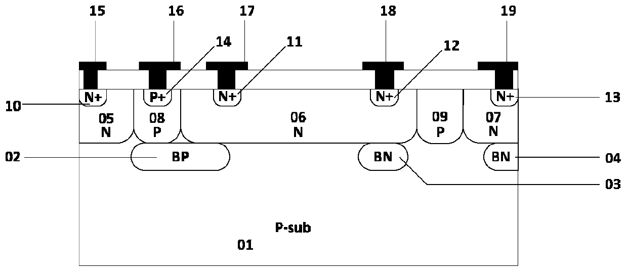
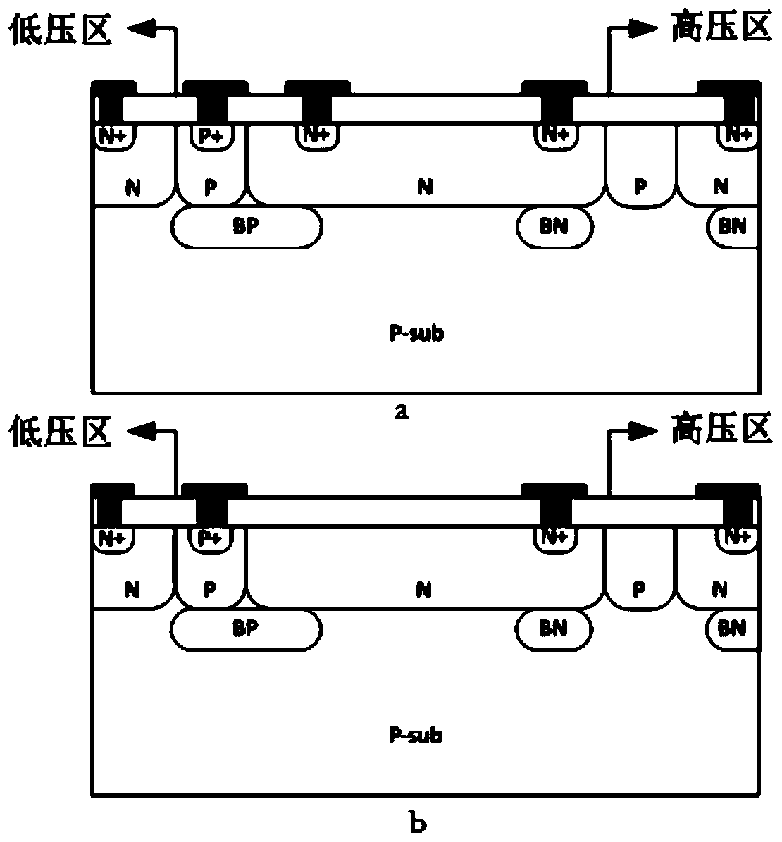
[0023] A bootstrap structure integrated on a high and low voltage isolation structure, including a first doped type substrate 01 that doubles as a high and low voltage isolation structure substrate, and a second doped type drift region 06 that doubles as a high and low voltage isolation structure drift region And the first doped type substrate contact well 08 which doubles as the high and low voltage isolation structure substrate contact well 08 is provided with the first doped type contact region as the substrate contact electrode in the first doped type substrate contact well 08 14. A bootstrap structure positive electrode and a bootstrap structure negative electrode are respectively provided on the drift region 06 of the second doping type, and the positive electrode of the bootstrap structure is a second electrode set in the drift region 06 of the second doping type The doping type contact region 11, the bootstrap structure negative electrode is another second doping type c...
Embodiment 2
[0027] A bootstrap circuit based on the bootstrap structure, including a bootstrap structure and a bootstrap capacitor 20, the bootstrap structure includes a first doping type substrate 01 that doubles as a high and low voltage isolation structure substrate, and a high The drift region 06 of the second doping type in the drift region of the low-voltage isolation structure and the substrate contact well 08 of the first doping type double as the substrate contact well of the high-voltage isolation structure are characterized in that the substrate contact well 08 of the first doping type The well 08 is provided with a first doping type contact region 14 as a substrate contact electrode, and a bootstrap structure positive electrode and a bootstrap structure negative electrode are respectively provided on the second doping type drift region 06, and the bootstrap structure The positive electrode is a second doping type contact region 11 arranged in the drift region 06 of the second d...
PUM
 Abstract
Description
Claims
Application Information
 - R&D
- Intellectual Property
- Life Sciences
- Materials
- Tech Scout
- Unparalleled Data Quality
- Higher Quality Content
- 60% Fewer Hallucinations
Browse by: Latest US Patents, China's latest patents, Technical Efficacy Thesaurus, Application Domain, Technology Topic, Popular Technical Reports.
© 2025 PatSnap. All rights reserved.Legal|Privacy policy|Modern Slavery Act Transparency Statement|Sitemap|About US| Contact US: help@patsnap.com


