
Via circuit of switching power domain parallel interface to normally open power domain parallel interface

A technology of switching power supply and interface circuit, which is applied in the direction of logic circuit interface device, logic circuit connection/interface layout, electrical digital data processing, etc., and can solve the problems of increasing area cost, large number of circuits, and reducing system performance, etc.

Inactive Publication Date: 2018-03-23
SHANGHAI HUAHONG INTEGRATED CIRCUIT +1
View PDF2 Cites 4 Cited by
  • Summary
  • Abstract
  • Description
  • Claims
  • Application Information

AI Technical Summary

Problems solved by technology

[0003] The defect of above-mentioned implementation mode is: the one, when transmitting data, system bus is in busy state, can not carry out other operation again, has reduced the performance of system; For the levelshifter) the number of circuits is large, which increases the area cost

Method used


Image

  • Via circuit of switching power domain parallel interface to normally open power domain parallel interface
  • Via circuit of switching power domain parallel interface to normally open power domain parallel interface

Examples


Embodiment Construction

[0011] Below in conjunction with accompanying drawing and specific embodiment the present invention is described in further detail:

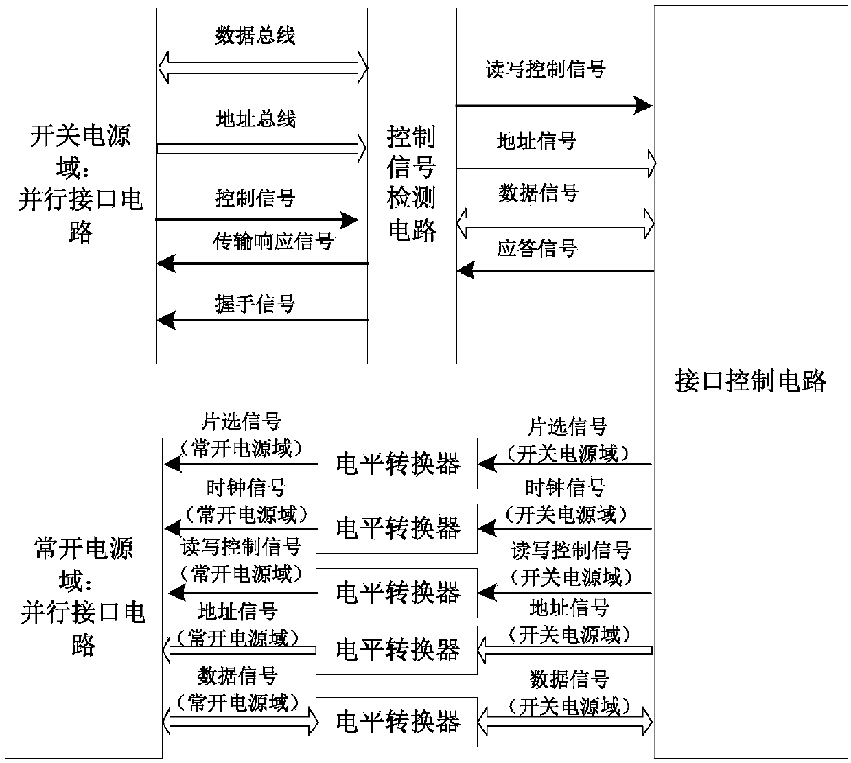
[0012] figure 1 It is the circuit principle diagram of the present invention, mainly composed of a control signal detection circuit and an interface control circuit. The control signal detection circuit mainly detects read and write signals, and latches valid data and addresses. The interface control circuit is mainly used to generate a response signal for a transmission

[0013] figure 2 It is a circuit realization block diagram of the present invention, and the signal description in the figure is as follows:

[0014] Control signal: It is the control signal of the high-performance system bus (hereinafter referred to as AHB bus) interface, including clock signal hclk, reset signal hreset_n, address bus haddr, strobe signal hsel, transmission length signal hsize, read and write control signal hwrite, Transmission type signal htrans, write dat...


PUM


Abstract

The invention discloses a via circuit of a switching power domain parallel interface to a normally open power domain parallel interface. The via circuit comprises a control signal detection circuit and an interface control circuit. A control signal detection module is connected with the switching power domain parallel interface through data, an address bus, control signals, transmission response signals, and handshaking signals. The control signal detection circuit detects reading-writing control signals, and latches effective data and addresses. In the interface control circuit, a response signal is set, and the response signal is sent to the control signal detection module when data transmission is completed, and the interface control circuit controls the handshaking signals of the signal detection module. Through the interface control circuit and the control signal detection circuit, the number of control signals of a normally open voltage domain interface circuit is reduced, the number of level shifters inserted between two power domains is reduced, and area is saved. Also, in the period of data transmission, data transmission is realized through the handshaking signals, a system bus is not occupied, and performance of the system is improved.

Description

technical field [0001] The invention relates to a switching circuit, in particular to a circuit for realizing interface communication between different power domains. Background technique [0002] In the low-power design, the SOC modules are divided into multiple voltage domains, and the driving capabilities of different voltage domains will be different, resulting in the limitation of the operating frequency in different voltage domains, and in different voltage domains. Each digital module needs to frequently interact with data. One way to achieve this is to increase the data writing completion flag, and the processor CPU can judge whether the writing is successful by querying the flag, and requires each write to the module After that, the flag must be queried. [0003] The defect of above-mentioned realization mode is: the one, when transmitting data, system bus is in busy state, can not carry out other operation again, has reduced the performance of system; For the lev...

Claims


Application Information

Patent Timeline
IPC IPC(8): G06F13/42G06F15/78H03K19/0175
CPCG06F13/4286G06F15/7807H03K19/017509Y02D10/00
Inventor 呼立展汤晓岚王吉健
Owner SHANGHAI HUAHONG INTEGRATED CIRCUIT
Learn More