
Three-dimensional memory with double-step structure and its formation method

A memory, double-step technology, used in semiconductor devices, electrical solid-state devices, electrical components, etc., can solve problems such as critical dimensions and contour control difficulties, and achieve the effect of reducing challenges and expanding storage capacity

Active Publication Date: 2019-01-29
YANGTZE MEMORY TECH CO LTD
View PDF3 Cites 0 Cited by
  • Summary
  • Abstract
  • Description
  • Claims
  • Application Information

AI Technical Summary

Problems solved by technology

And the three-dimensional memory has gradually developed from 32 word line (Word Line) layers to 48, 64, 96, 128, 256 or even more, which means that the horizontal and vertical cell dimensions of the three-dimensional memory have been expanded, increasing storage capacity; however, with the horizontal and vertical expansion of the unit dimension of the three-dimensional memory, for subsequent processes (such as: photolithography, etching, etc.) and feature structures (such as: holes, trenches, connections, etc. ) aspect ratio control brings great challenges; especially in the case of high selectivity of oxide, nitride, polysilicon, etc., the critical dimension and profile control of each structure becomes more and more difficult

Method used


Image

  • Three-dimensional memory with double-step structure and its formation method
  • Three-dimensional memory with double-step structure and its formation method
  • Three-dimensional memory with double-step structure and its formation method

Examples


Embodiment 1

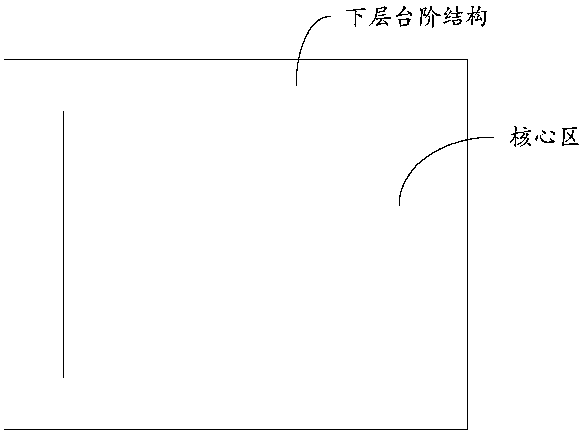
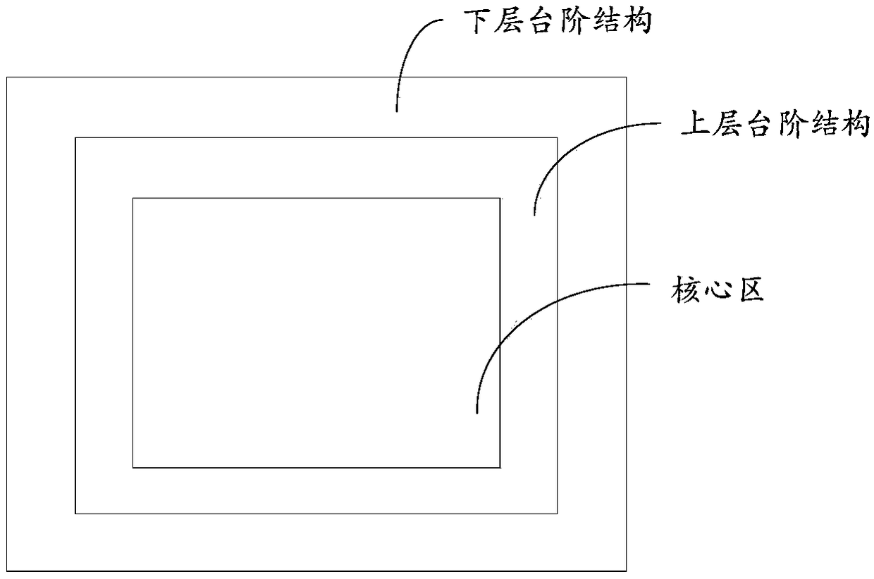
[0040] According to an embodiment of the present invention, a method for forming a three-dimensional memory with a double-step structure is provided, such as Figure 1 to Figure 9 shown, including:

[0041] provide the substrate;

[0042] A first stacked structure is formed on the substrate, and a lower step area, a lower coverage area, and a lower trench via are respectively formed on the first stack structure to obtain a lower step structure; the lower coverage area covers the lower step area and the first stack The upper surface of the structure, and the part covering the upper surface of the first laminated structure is used as the condensation layer;

[0043] A second stacked structure is formed on the lower stepped structure, and an upper stepped area, an upper covered area and an upper trench via are respectively formed on the second stacked structure to obtain an upper stepped structure; the upper covered area covers the upper stepped area.

[0044] According to an e...

Embodiment 2

[0065] According to an embodiment of the present invention, a three-dimensional memory with a double-step structure is provided, including:

[0066] Substrate;

[0067] The lower step structure on the substrate;

[0068] an upper step structure on a lower step structure;

[0069] Wherein, the lower stepped structure includes: the first stacked structure, and the lower stepped area, the lower covered area and the lower channel via hole formed on the first stacked structure; the lower covered area includes the first stacked structure covered Concrete layer on the surface;

[0070] The upper stepped structure includes: a second stacked structure, and an upper stepped area, an upper covering area and an upper channel via hole respectively formed on the second stacked structure.

[0071] According to an embodiment of the present invention, the via holes of the lower layer channel correspond one-to-one with the via holes of the upper layer channel and penetrate through each other...


PUM


Abstract

The invention discloses a three-dimensional memory with a double-step structure and a forming method thereof, belonging to the technical field of semiconductors. The method includes: providing a substrate; forming a first laminated structure on the substrate, respectively forming a lower layer step region, a lower layer covering region and a lower layer channel via hole on the first layer structure to obtain a lower layer step structure; and the lower layer covering The region covers the lower step region and the upper surface of the first stacked structure, and the part covering the upper surface of the first stacked structure is used as a condensation layer; a second stacked structure is formed on the lower stepped structure, and the second stacked structure The upper layer step area, the upper layer covering area and the upper layer trench via hole are respectively formed on the upper layer to obtain the upper layer step structure; and the upper layer covering area covers the upper layer step area. In the present invention, not only the storage capacity of the three-dimensional memory is expanded, but also it is beneficial to control the key dimensions and contours of each structure in the subsequent process, which greatly reduces the challenges in the process.

Description

technical field [0001] The invention relates to the technical field of semiconductors, in particular to a three-dimensional memory with a double-step structure and a forming method thereof. Background technique [0002] Flash memory is a non-volatile memory and a special structure of electrically erasable and programmable read-only memory. Its operating principle is to control the switch of the gate channel by changing the critical voltage of the transistor or memory cell to achieve The purpose of storing data so that the data stored in the memory will not disappear due to power interruption. Flash memory has become a hotspot in the research of non-volatile memory due to its convenience, high storage density, and good reliability. Since the first flash memory product came out in the 1980s, with the development of technology and the storage needs of various electronic products, flash memory has been widely used in mobile and communication devices such as mobile phones, noteb...

Claims


Application Information

Patent Timeline
Patent Type & Authority Patents(China)
IPC IPC(8): H01L27/11551H01L27/11578H10B41/20H10B43/20
CPCH10B41/20H10B43/20
Inventor 肖莉红胡禺石陶谦周玉婷
Owner YANGTZE MEMORY TECH CO LTD
Learn More