Semiconductor templates and fabrication methods

A semiconductor and template technology, applied in the field of semiconductor template production

Inactive Publication Date: 2018-02-16
SEREN PHOTONICS
View PDF4 Cites 0 Cited by
  • Summary
  • Abstract
  • Description
  • Claims
  • Application Information

AI Technical Summary

Problems solved by technology

However, the problem with this approach is that a substantial portion of the basal stacking faults in the crystal structure of the semiconductor pillar still grow outward from the sides of the pillar and into the main semiconductor layer.

Method used


Image

  • Semiconductor templates and fabrication methods
  • Semiconductor templates and fabrication methods
  • Semiconductor templates and fabrication methods

Examples


Embodiment Construction

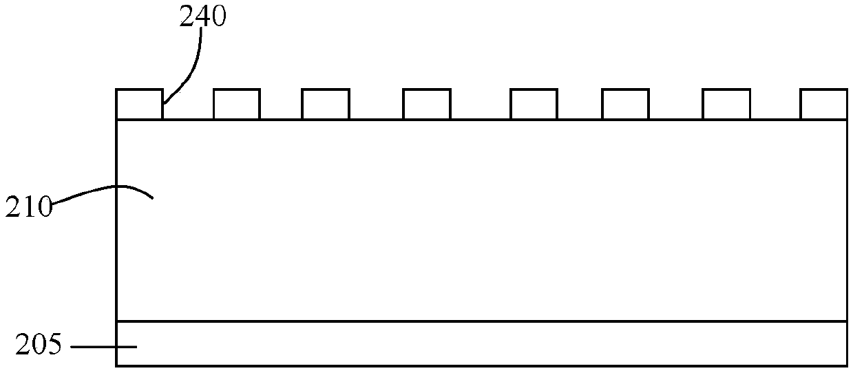
[0049] see Figure 1a , the first step in fabricating a semiconductor template is to provide a suitable semiconductor wafer 201 . Wafer 201 is conventional and consists of a substrate 205, in this case comprising a layer of sapphire, on top of which is a semiconductor layer 210 formed of gallium nitride (GaN). Other materials can be used. For example, the substrate can be silicon (flat or patterned) or silicon carbide (flat or patterned). The semiconductor may be another suitable material, for example another group III nitride such as indium gallium nitride (InGaN) or aluminum gallium nitride (AlGaN) or indium nitride (InN) or aluminum nitride (AlN). Semiconductor wafers are semipolar. Specifically, in this embodiment, the GaN is oriented such that its top surface parallel to the plane of the substrate (referred to herein as the horizontal plane) is in the (11-22) plane. A buffer layer or a nucleation layer, such as high-temperature AlN or thin low-temperature GaN or thin ...


PUM


Abstract

A method of making a semi-polar semiconductor template comprises providing a semi-polar semiconductor wafer; etching the semiconductor wafer to form a regular semiconductor structure comprising a plurality of semiconductor regions (260) with a plurality of gaps between the regions, each of the regions (260) having a sidewall facing a respective one of the gaps, and growing semiconductor material over the semiconductor structure. The semiconductor material has a preferential growth direction (c) in which growth proceeds most rapidly from each of the sidewalls, and each of the sidewalls has at least a part which faces a vertical centre line of the respective one of the gaps so that growth in the preferential direction from said part extends towards said vertical centre line.

Description

technical field [0001] The present invention relates to semiconductor templates and methods of manufacturing semiconductor templates. In particular, the invention relates to the production of semiconductor templates with high-quality crystal structures. Templates can be used, for example, in the formation of light emitting diodes and solid state lasers. Background technique [0002] Our earlier patent application PCT / GB2012 / 050458 describes a method of growing semiconductor crystalline structures, such as GaN crystalline structures, in which irregular arrays of pillars, also known as nanopillars, micropillars, rods or pillars, are formed and then A layer of semiconducting material is grown laterally from the side of the pillar and then grown on top of the pillar with a mask layer that prevents growth on top of the pillar, which helps prevent threading, edge and mixed dislocations from the top of the pillar upwards extension. The problem with this approach, however, is tha...

Claims


Application Information

Patent Timeline
Patent Type & Authority Applications(China)
IPC IPC(8): H01L21/02
CPCH01L21/02458H01L21/02516H01L21/0254H01L21/02603H01L21/02609H01L21/0265
Inventor 王涛
Owner SEREN PHOTONICS
Why Eureka
Try Eureka