
Method for manufacturing an organic light-emitting device and the organic light-emitting device

A technology of an organic light-emitting device and a manufacturing method, which is applied in the manufacture of organic light-emitting devices and the field of organic light-emitting devices, can solve the problems of poor lifespan, rapid voltage rise, poor stability and the like of organic light-emitting devices

Active Publication Date: 2019-04-30
EVERDISPLAY OPTRONICS (SHANGHAI) CO LTD
View PDF3 Cites 0 Cited by
  • Summary
  • Abstract
  • Description
  • Claims
  • Application Information

AI Technical Summary

Problems solved by technology

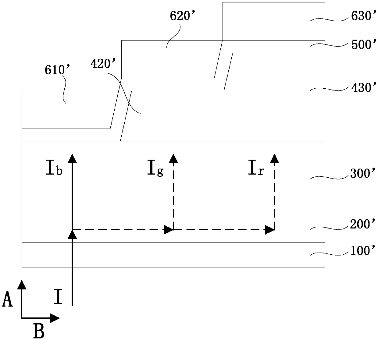
However, the thinning of the hole injection layer 200' will lead to poor stability, causing the voltage of the organic light-emitting device to rise rapidly during the lighting process, making the life of the organic light-emitting device worse.

Method used


Image

  • Method for manufacturing an organic light-emitting device and the organic light-emitting device
  • Method for manufacturing an organic light-emitting device and the organic light-emitting device
  • Method for manufacturing an organic light-emitting device and the organic light-emitting device

Examples


Embodiment Construction

[0048] Example embodiments will now be described more fully with reference to the accompanying drawings. Example embodiments may, however, be embodied in many forms and should not be construed as limited to the embodiments set forth herein; rather, these embodiments are provided so that this disclosure will be thorough and complete, and will fully convey the concept of example embodiments to those skilled in the art. The same reference numerals denote the same or similar structures in the drawings, and thus their repeated descriptions will be omitted.

[0049] The described features, structures, or characteristics may be combined in any suitable manner in one or more embodiments. In the following description, numerous specific details are provided in order to give a thorough understanding of embodiments of the invention. However, those skilled in the art will appreciate that the technical solutions of the present invention may be practiced without one or more of the specific...


PUM


Abstract

The invention provides a method for manufacturing an organic light-emitting device and the organic light-emitting device, wherein the method includes: providing a transparent conductive layer; and vapor-depositing at least one structural layer on the transparent conductive layer in a magnetic field, and the structural layer is empty One of hole injection layer, hole transport layer, electron blocking layer, light-emitting layer, hole blocking layer, electron transport layer, and electron injection layer. The molecular chains of the structural layer are highly oriented along the direction of magnetic field lines of magnetic field. The present invention can increase the lateral resistance of the hole injection layer without reducing the thickness of the hole injection layer, thereby isolating the current in the hole injection layer from migrating from the blue pixel area to the green or red pixel area under low brightness , improve OLED low-grayscale color shift, and increase the service life of organic light-emitting devices.

Description

technical field [0001] The invention relates to the field of display devices, in particular to a method for manufacturing an organic light emitting device and the organic light emitting device. Background technique [0002] During the OLED manufacturing process, crystal anisotropy and carrier mobility are important factors to be considered. [0003] The anisotropy of the crystal means that along different directions of the crystal lattice, the periodicity and density of atomic arrangement are not the same, which leads to different physical and chemical properties of the crystal in different directions, which is the anisotropy of the crystal. The anisotropy of the crystal can be manifested in the elastic modulus, hardness, fracture resistance, yield strength, thermal expansion coefficient, thermal conductivity, resistivity, electric displacement vector, electric polarization, magnetic susceptibility and refractive index in different directions of the crystal. is different. ...

Claims


Application Information

Patent Timeline
Patent Type & Authority Patents(China)
IPC IPC(8): H01L51/50H01L51/56
CPCH10K50/18H10K50/17H10K71/00
Inventor 欧阳攀
Owner EVERDISPLAY OPTRONICS (SHANGHAI) CO LTD
Learn More