Micro LED device and preparation method therefor, and display apparatus

A LED device, miniature technology, applied in the direction of semiconductor devices, electrical components, circuits, etc., can solve the problems of high cost and long transfer process time

Active Publication Date: 2018-02-09
INTERFACE TECH CHENGDU CO LTD +2
View PDF6 Cites 9 Cited by
  • Summary
  • Abstract
  • Description
  • Claims
  • Application Information

AI Technical Summary

Problems solved by technology

[0003] Based on this, it is necessary to address the problems of long time and high cost of the micro-LED transfer process, and to provide a method for preparing a micro-LED device, comprising the following steps: preparing nano-LED particles; providing nano-conductive particles and an adhesive, and placing the nano-LED Mixing the particles, the

Method used


Image

  • Micro LED device and preparation method therefor, and display apparatus
  • Micro LED device and preparation method therefor, and display apparatus
  • Micro LED device and preparation method therefor, and display apparatus

Examples


preparation example Construction

[0017] A method for preparing a micro-LED device, comprising the following steps:

[0018] S1: preparing nano-LED particles;

[0019] S2: providing nano conductive particles and an adhesive, mixing the nano LED particles, the nano conductive particles and the adhesive to obtain a first mixture;

[0020] S3: providing a substrate, and forming a first electrode layer on the substrate;

[0021] S4: coating the first mixture on the first electrode layer, and performing curing treatment to form a composite layer;

[0022] S5: forming a second electrode layer on the composite layer to obtain the micro LED device.

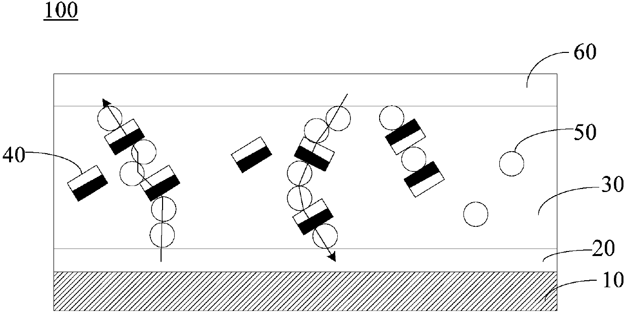
[0023] see figure 1 , the micro LED device 100 prepared by the above method includes the substrate 10, the first electrode layer 20, the composite layer 30 and the second electrode layer 60 which are stacked in sequence, and the micro LED device 100 also includes the substrate dispersed in the composite layer 30. Nano LED particles 40 and nano conductive particles 50 ...


PUM


Abstract

The invention relates to a preparation method of a micro LED device. The preparation method comprises the following steps of preparing nanometer LED particles; providing nanometer conductive particlesand an adhesive, and performing mixing on the nanometer LED particles, the nanometer conductive particles and the adhesive to obtain a first mixture; providing a substrate, and forming a first electrode layer on the substrate; coating the first electrode layer with the first mixture and performing curing treatment to form a composite layer; and forming a second electrode layer on the composite layer to obtain the micro LED device. By virtue of the preparation method of the micro LED device, the transferring and packaging difficulty of the nanometer LED particles can be lowered, the productionefficiency is improved and the production cost is lowered.

Description

technical field [0001] The invention relates to the field of display technology, in particular to a micro light-emitting diode device, a preparation method thereof, and a display device. Background technique [0002] Compared with the existing liquid crystal display (LCD) and organic light-emitting diode display (OLED), micro-LED devices have the advantages of high display brightness, fast response speed, and long life. Dimensions are usually on the order of microns. After micro-LEDs are obtained by epitaxial growth on substrates such as sapphire or silicon carbide, how to transfer and integrate the micro-LEDs onto the target substrate is a technical difficulty in preparing micro-LED devices. In order to ensure that the polarities of a large number of micro-LEDs are consistent during the transfer process, the existing solutions usually take a long time and cost a lot. Contents of the invention [0003] Based on this, it is necessary to address the problems of long time a...

Claims


Application Information

Patent Timeline
IPC IPC(8): H01L33/26H01L33/00
CPCH01L33/005H01L33/26
Inventor 黄功杰
Owner INTERFACE TECH CHENGDU CO LTD
Why Eureka
Try Eureka