
Device for carrier tape bagging and cover tape offset correction after chip package test and process thereof

A technology of chip packaging and deviation correction device, which is applied in packaging, packaging machines, packaging protection, etc., can solve the problems of cover tape detachment and wire drawing, and achieve the effects of avoiding deviation, obvious deviation correction effect, and reducing the volume of components

Active Publication Date: 2018-02-06
CHANGJIANG ELECTRONICS TECH CHUZHOU
View PDF6 Cites 1 Cited by
  • Summary
  • Abstract
  • Description
  • Claims
  • Application Information

AI Technical Summary

Problems solved by technology

[0006] In view of the problems in the prior art that the position of the chip on the suction nozzle is not aligned with that of the POCKET that is entering the carrier tape, it is easy to cause warped feet and the cover tape is disengaged and drawn due to the offset of the cover tape. Carrier tape into bag and cover tape deflection correcting device and its technology

Method used


Image

  • Device for carrier tape bagging and cover tape offset correction after chip package test and process thereof
  • Device for carrier tape bagging and cover tape offset correction after chip package test and process thereof
  • Device for carrier tape bagging and cover tape offset correction after chip package test and process thereof

Examples


Embodiment 1

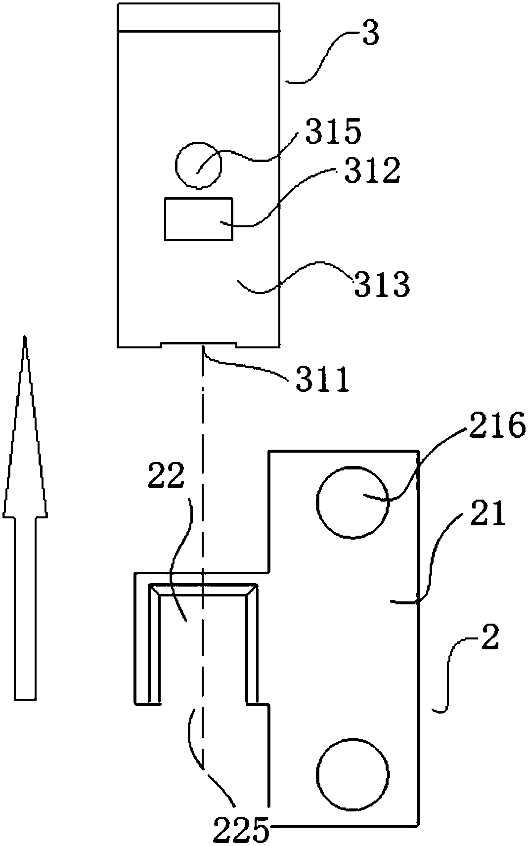
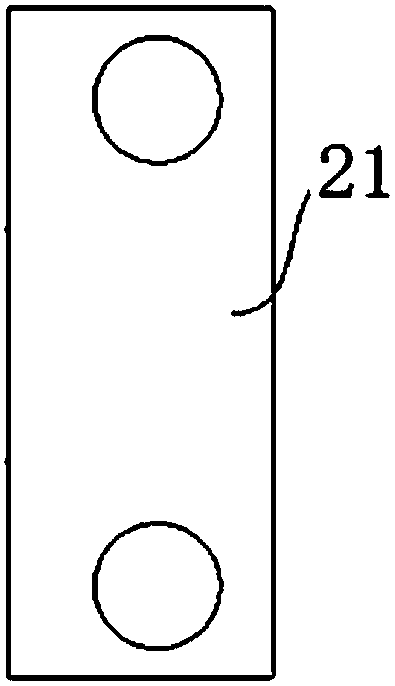
[0059] After the chip packaging test of this embodiment, the carrier tape is put into the bag and the cover tape deflection correction device, such as figure 1 As shown, it includes the carrier tape bagging mechanism 2 and the cover tape offset prevention mechanism 3 arranged in the process order, wherein: as Figure 4 As shown, the carrier tape pocketing mechanism 2 includes a square pressing plate 21 and a braiding window 22 extending from the middle of the square pressing plate 21 to the running direction of the carrier tape; the square pressing plate 21 and the braiding window 22 are fixedly connected as one, through The braiding window guides the suction nozzle to put the chip into the POCKET of the carrier tape, which prevents the pin from touching the edge of the POCKET and causing the pin to become warped; the bottom of the braiding window 22 is opened as an outer opening 225, so that Install other devices in the installation space, such as detection devices; Figure...

Embodiment 2

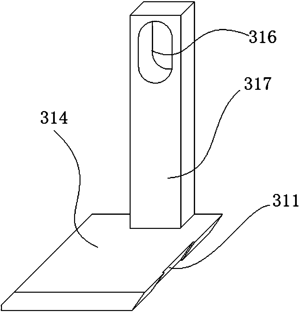
[0061] The carrier tape of the present embodiment after the chip packaging test is put into the bag and the cover tape deflection correction device, the basic structure is the same as that of embodiment 1, the difference and improvement are that the shape and size of the bottom of the braiding window 22 are consistent with the opening of the bag of the carrier tape, Both are 3.3X3.2mm, forming a straight drop microchannel of the chip to avoid secondary offset when the chip is placed; the soft connection is realized through the cooperation of the elastic mechanism and the directional track mechanism, the elastic mechanism achieves the purpose of buffering, and the directional track realizes The purpose of avoiding offset; the depth of the cover tape groove 311 is greater than the thickness of the cover tape. In this embodiment, the platen groove 311 is 10dmm deep, and the cover tape is 6dmm thick, so as to ensure that the cover tape does not shake back and forth in the cover tape...

Embodiment 3

[0063] The basic structure of the carrier tape into the bag and the cover tape deflection correcting device after the chip package test of this embodiment is the same as that of Embodiment 2, the differences and improvements are as follows: Figure 5 As shown, the braiding window 22 includes a square area 221 at the bottom and a receiving area 222 at the upper part. The angle of chip placement is corrected through the receiving interface to prevent the pin from touching the edge of the POCKET. The thickness ratio of the two is 2-4:6- 8. In this embodiment, the thickness ratio of the two is 3:7, and the thickness of the receiving area is larger, almost twice as large, providing a relatively large operating space for deviation correction; the upper surface of the pressure plate 31 is fixed with a vertical pressure plate public rail rod 312; the bottom surface of the support 32 is provided with a support female rail hole 321 that cooperates with the pressing plate male rail rod 31...


PUM


Abstract

The invention discloses a device for carrier tape bagging and cover tape offset correction after a chip package test and a process thereof, belonging to the technical field of chip packaging. The device comprises a carrier tape bagging mechanism and a cover tape offset preventing mechanism arranged in a process order. The carrier tape bagging mechanism comprises a square pressing plate and a taping window which is extended outwards from the middle of the square pressing plate to the running direction of the carrier tape, wherein the square pressing plate and the tapingwindow are fixedly connected in to one, and the bottom of the taping window is opened to the outside. The cover tape offset preventing mechanismcomprises apressing plate, a bracket, and a fixing frame; the pressing plate, thebracket, wherein the fixing frame are connected in turn in a soft connection mode, a cover tape groove is formed in the side of the pressing plate for guiding the running direction of the cover tape,the width of the cover tape groove is the same as the cover tape, and the vertical center lines of the taping window and the cover tape groove are in the same plane. The device is provided with the anti-warping leg taping window for the nozzle to accurately insert a chip into a carrier tape bag, improves the original hard connection into soft connection, and is capable of fine adjustment to achieve the purpose of effectively preventing the offset of the cover tape.

Description

technical field [0001] The invention relates to the technical field of chip packaging, in particular to a device for correcting carrier tape into bag and cover tape after chip packaging and testing, and a technology thereof. Background technique [0002] Such as figure 2 As shown, the taping station designed by the original equipment has no window, but a square platen (21) that presses the carrier tape is installed on the right side, the thickness is 1mm, and the suction nozzle is 2.9X2.8mm (wherein 2.8mm represents the lead of the product). The chip product of the span between feet) enters the 3.3X3.2mm carrier tape POCKET (can be translated as a cloth bag) with the drop of the suction nozzle, and the 3.2mm of the carrier tape POCKET is the width, and the product with a width of 2.8mm enters the In a POCKET with a width of 3.2mm, the allowable error is only plus or minus 0.2mm from left to right. Due to various reasons, the product on the suction nozzle may deviate beyond ...

Claims


Application Information

Patent Timeline
Patent Type & Authority Applications(China)
IPC IPC(8): B65B35/18B65B65/00B65B15/04B65B57/18
CPCB65B15/04B65B35/18B65B57/18B65B65/00
Inventor 李国祥汪阳胡惠民邱冬冬
Owner CHANGJIANG ELECTRONICS TECH CHUZHOU
Learn More