
Three-dimensional (3D) NAND fabrication method for preventing silicon epitaxial growth (SEG) from being damaged and obtained 3D NAND flash memory

An oxidation method and substrate technology, applied to electrical components, electrical solid devices, circuits, etc., can solve problems such as 3D structure collapse, SEG damage, BSG failure, etc., to achieve the effect of preventing collapse, reducing failure rate, and expanding the window

Active Publication Date: 2018-02-02
YANGTZE MEMORY TECH CO LTD
View PDF4 Cites 6 Cited by
  • Summary
  • Abstract
  • Description
  • Claims
  • Application Information

AI Technical Summary

Problems solved by technology

[0021] Micrographs of damage to SEG after phosphoric acid etching in the prior art are shown as Figure 7 shown; and fracture and collapse of 3D structure or failure of BSG in subsequent BSG oxidation; yield loss greater than 90%

Method used


Image

  • Three-dimensional (3D) NAND fabrication method for preventing silicon epitaxial growth (SEG) from being damaged and obtained 3D NAND flash memory
  • Three-dimensional (3D) NAND fabrication method for preventing silicon epitaxial growth (SEG) from being damaged and obtained 3D NAND flash memory
  • Three-dimensional (3D) NAND fabrication method for preventing silicon epitaxial growth (SEG) from being damaged and obtained 3D NAND flash memory

Examples


Embodiment Construction

[0072] Exemplary embodiments of the present disclosure will be described in more detail below with reference to the accompanying drawings. Although exemplary embodiments of the present disclosure are shown in the drawings, it should be understood that the present disclosure may be embodied in various forms and should not be limited by the embodiments set forth herein. Rather, these embodiments are provided for more thorough understanding of the present disclosure and to fully convey the scope of the present disclosure to those skilled in the art.

[0073] In the interest of clarity, not all features of an actual implementation are described. In the following description, well-known functions and constructions are not described in detail since they would obscure the invention with unnecessary detail. It should be appreciated that in the development of any actual embodiment, numerous implementation details must be worked out to achieve the developer's specific goals, such as ch...


PUM


Abstract

The invention provides a three-dimensional (3D) NAND fabrication method for preventing silicon epitaxial growth (SEG) from being damaged and an obtained 3D NAND flash memory. The method comprises thesteps of generating a grid hard mask oxide on a surrounding region and forming an oxide film layer on a back surface of a substrate by a low-temperature oxidization method during the fabrication process of a surrounding region device, and controlling a cleaning process of the back surface of the substrate so that the hard mask oxide on the back surface of the substrate is reserved to a channel hole fabrication process. By the method, charge generation is prevented, electrochemical reaction during the phosphorous etching process is prevented so as to damage the SEG, the collapse of a 3D structure can be further prevented, the BSG failure rate is reduced, and higher produce yield is obtained.

Description

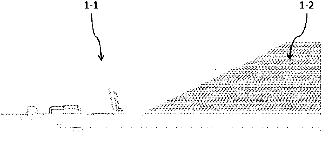
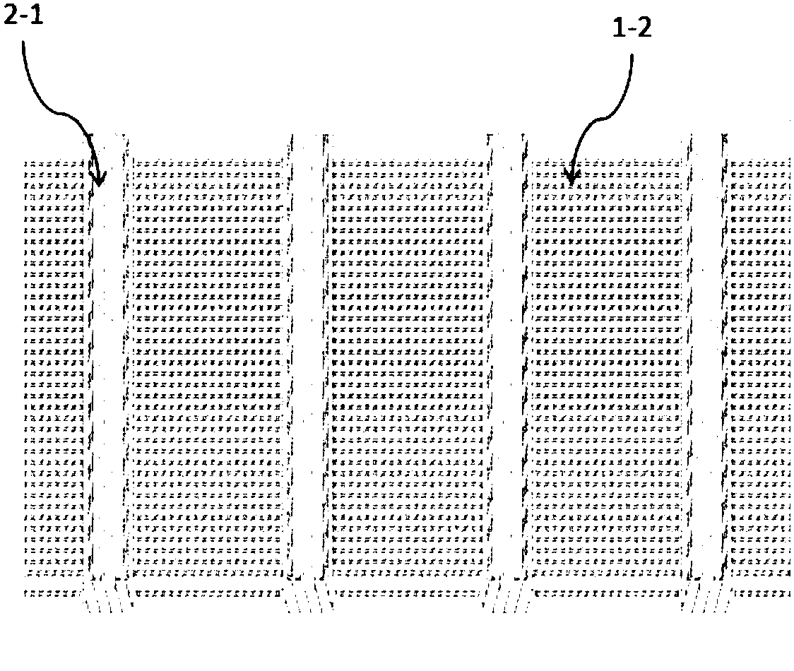
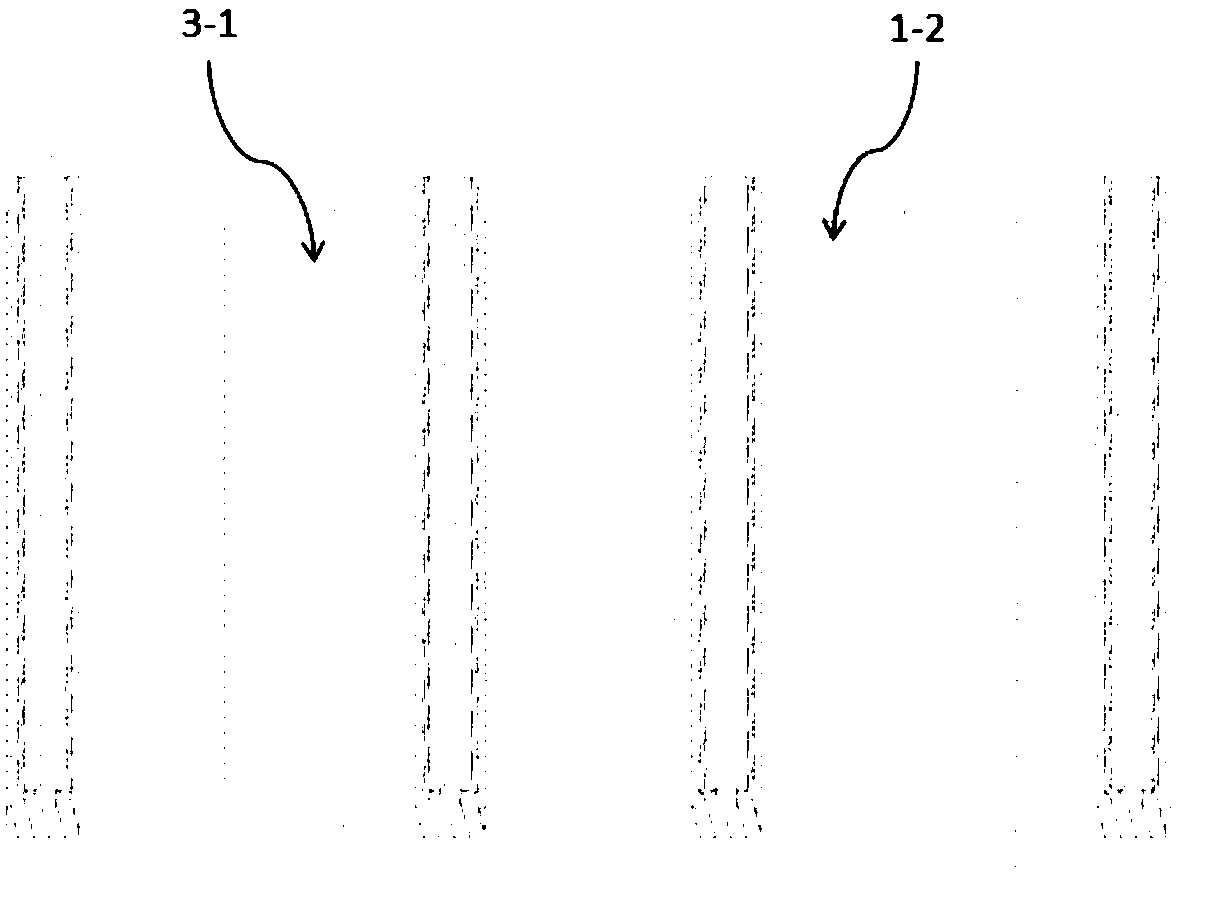
technical field [0001] The invention relates to the field of semiconductor manufacturing, in particular to a 3D NAND preparation method for preventing SEG damage and the obtained 3D NAND flash memory. Background technique [0002] In order to improve the density of memory devices, the industry has made extensive efforts to develop methods of reducing the size of two-dimensionally arranged memory cells. As the size of memory cells in two-dimensional (2D) memory devices continues to shrink, signal collisions and interference can increase significantly, making it difficult to perform multi-level cell (MLC) operations. In order to overcome the limitations of 2D memory devices, research on memory devices with a three-dimensional (3D) structure has gradually heated up this year, and integration density is increased by three-dimensionally arranging memory cells on a substrate. [0003] 3D NAND flash memory, such as Figure 1-3 As shown, it includes a peripheral device region 1-1 a...

Claims


Application Information

Patent Timeline
IPC IPC(8): H01L27/11524H01L27/11526H01L27/11551H01L27/1157H01L27/11573H01L27/11578H10B41/35H10B41/20H10B41/40H10B43/20H10B43/35H10B43/40
CPCH10B41/35H10B41/40H10B41/20H10B43/35H10B43/40H10B43/20
Inventor 陆智勇隋翔宇王香凝唐兆云江润峰
Owner YANGTZE MEMORY TECH CO LTD
Learn More