Acidic copper plating solution, acidic copper plated product, and method for producing semiconductor device
An acid copper plating, polymer technology, applied in semiconductor/solid-state device manufacturing, semiconductor devices, semiconductor/solid-state device components and other directions, can solve problems such as increased manufacturing cost, wiring layer disconnection, increased heating process CMP process, etc. Achieve the effect of suppressing thermal expansion and realizing practical application
- Summary
- Abstract
- Description
- Claims
- Application Information
AI Technical Summary
Problems solved by technology
Method used
Image
Examples
Embodiment approach 1
[0039] In this embodiment, the acidic copper plating solution of the present invention will be described.
[0040]The acidic copper plating solution of the present invention is characterized in that it contains: a first additive composed of a cationic polymer; The second additive of at least one of the group consisting of dihydrate, ethylenethiourea, and part of the 2-mercapto-5-benzimidazole sulfonate of poly(diallyldimethylammonium chloride) and a third additive composed of an organic compound containing sulfur atoms, the copper concentration of the acidic copper plating solution is 10-60g / L, the sulfuric acid concentration is 10-200g / L, and contains chloride ions below 90mg / L.
[0041] The cationic polymer used as the first additive is not particularly limited as long as it has a cationic group in its molecule. Examples of cationic groups include primary amino groups, secondary amino groups, tertiary amino groups, and quaternary ammonium groups. Polymers containing primar...
Embodiment approach 2
[0051] In this embodiment, the acidic copper plating object obtained by electroplating using the acidic copper plating liquid of this invention is demonstrated.
[0052] The acidic copper-plated article of the present invention is characterized in that, compared with the conventional acidic copper-plated article, the lattice constant at room temperature is large, for example greater than The lattice constant of the acidic copper plating object of the present invention is preferably
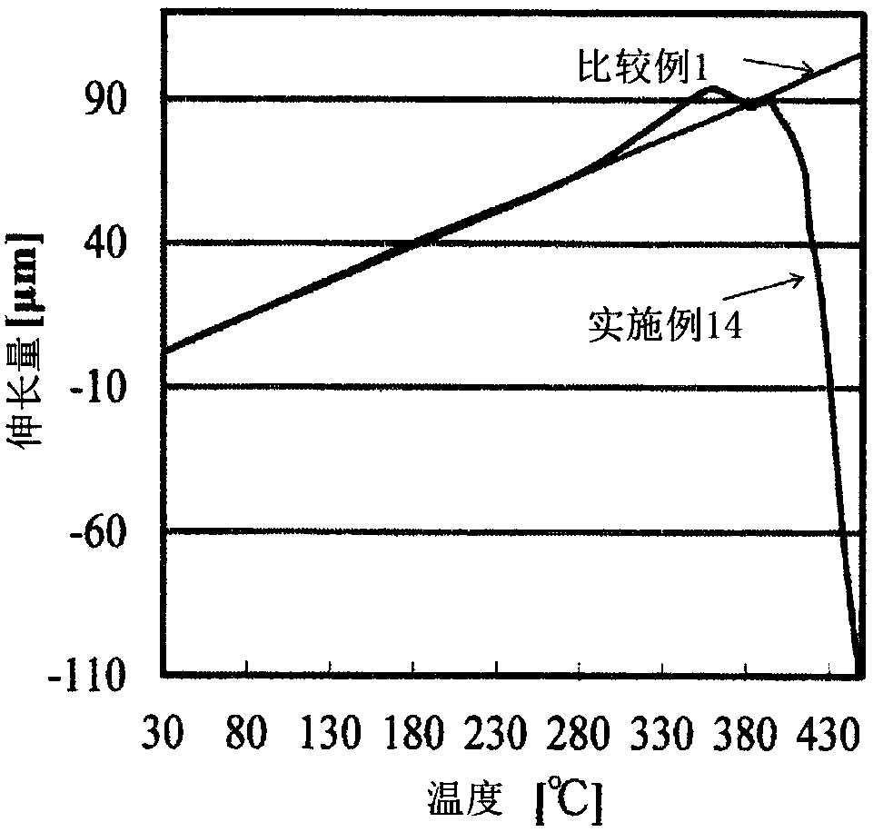
[0053] Furthermore, the linear expansion coefficient of the acidic copper plating material of this invention is smaller than the conventional acidic copper plating material. The linear expansion coefficient of conventional copper plating is 1.70×10 -5 / K, take a fixed value independent of temperature. On the other hand, the linear expansion coefficient of the acidic copper-plated material of this invention is smaller than the conventional copper plating at a certain temperature or more or a...
Embodiment approach 3
[0066] In this embodiment mode, a method of manufacturing a semiconductor device having a through-silicon electrode using the acidic copper plating solution of the present invention will be described.
[0067] The method of manufacturing a semiconductor device having a through-silicon electrode according to the present invention is characterized in that the step of producing the through-silicon electrode includes forming a non-through hole on the one main surface of a silicon substrate on which a transistor is formed. Step: A step of performing copper plating on at least the non-through hole by electroplating using the acidic copper plating solution described in claim 1; and polishing the other main surface of the silicon substrate to fill the The copper of the non-through hole is exposed, and the step of forming the silicon through-hole electrode is formed.
[0068] In addition, in this manufacturing method, in the step of performing copper plating, copper may be filled in th...
PUM
| Property | Measurement | Unit |
|---|---|---|
| diameter | aaaaa | aaaaa |
| depth | aaaaa | aaaaa |
| length | aaaaa | aaaaa |
Abstract
Description
Claims
Application Information
 - R&D
- Intellectual Property
- Life Sciences
- Materials
- Tech Scout
- Unparalleled Data Quality
- Higher Quality Content
- 60% Fewer Hallucinations
Browse by: Latest US Patents, China's latest patents, Technical Efficacy Thesaurus, Application Domain, Technology Topic, Popular Technical Reports.
© 2025 PatSnap. All rights reserved.Legal|Privacy policy|Modern Slavery Act Transparency Statement|Sitemap|About US| Contact US: help@patsnap.com


