A multi-channel high-speed optical module structure and processing method
A high-speed, optical module technology, applied in the field of optical modules, can solve problems such as affecting the wiring of radio frequency lines, and achieve the effect of good radio frequency effect
- Summary
- Abstract
- Description
- Claims
- Application Information
AI Technical Summary
Problems solved by technology
Method used
Image
Examples
Embodiment 1
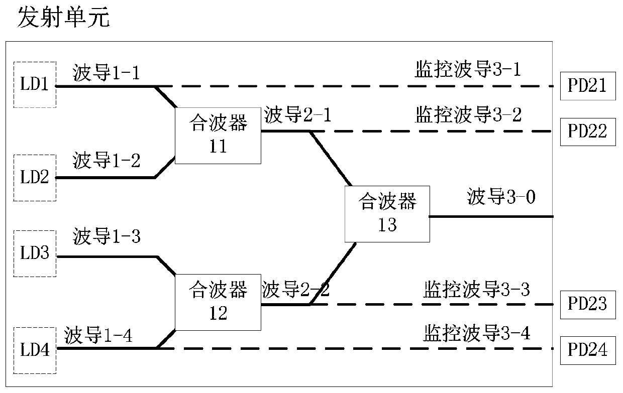
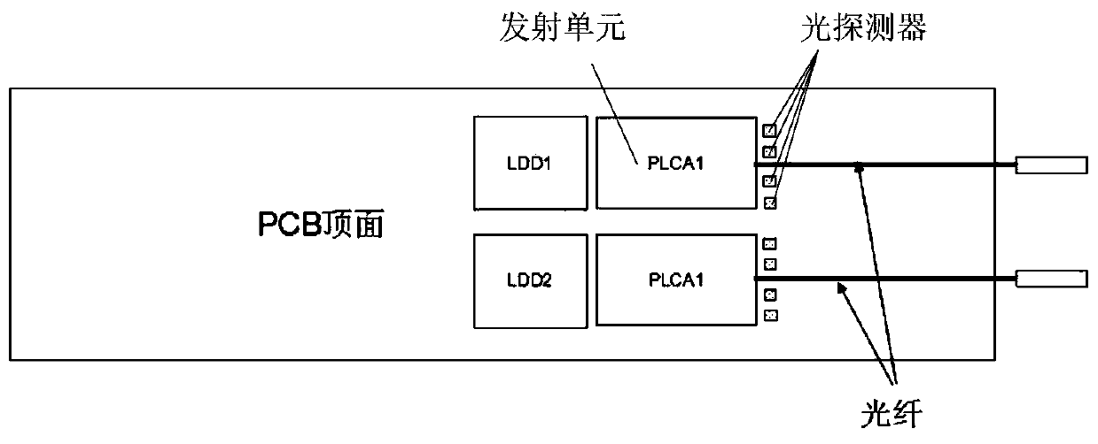
[0087] Embodiment 1 of the present invention provides a multi-channel high-speed optical module structure, such as figure 1 As shown, at least one transmitting unit is included, wherein the transmitting unit includes a first laser 1, a second laser 2, a third laser 3, a fourth laser 4, a first multiplexer 11, a second multiplexer 12, a third The multiplexer 13, the first photodetector 21, the second photodetector 22, the third photodetector 23 and the fourth photodetector 24, specifically:
[0088] The first laser 1 and the second laser 2 are respectively connected to the first wave combiner 11 through the first waveguide 1-1 and the second waveguide 1-2; wherein, relative to the horizontal direction, the first wave combiner 11 is located below the first laser 1 and above the second multiplexer 12;
[0089] The third laser 3 and the fourth laser 4 are respectively connected to the second wave combiner 12 through the third waveguide 1-3 and the fourth waveguide 1-4; wherein, r...
Embodiment 2
[0108] After providing a multi-channel high-speed optical module structure as described in Embodiment 1, the embodiment of the present invention focuses on how to complete the manufacture of the PLC unit used in Embodiment 1, such as Figure 14 As shown, the preparation method includes:
[0109] In step 201, a waveguide base material is grown on the wafer, so that the thickness of the waveguide base material reaches the preset waveguide setting parameters; wherein, the waveguide base material includes a waveguide lower cladding layer.
[0110] In step 202, a photoresist is coated, and the first waveguide 1-1, the second waveguide 1-2, the fifth waveguide 2-1, the sixth waveguide 2-2, the light output waveguide 3-0, the first Graphics of a monitoring waveguide 3-1, a second monitoring waveguide 3-2 and a third monitoring waveguide 3-3; wherein, at the junction of the first waveguide 1-1, the second waveguide 1-2 and the fifth waveguide 2-1 Photocut the pattern of the first mul...
Embodiment 4
[0128] Corresponding to Embodiment 3, the embodiment of the present invention also provides a method for manufacturing a PLC in a multi-channel high-rate optical module, and the manufactured PLC is used in the structure of the multi-channel high-rate optical module described in Embodiment 3, such as Figure 18 As shown, the preparation method includes:
[0129] In step 301, a waveguide base material is grown on the wafer, so that the thickness of the waveguide base material reaches the preset parameters set for the first waveguide layer; wherein, the waveguide base material includes a waveguide lower cladding layer.
[0130] In step 302, a photoresist is applied, and patterns of the second monitoring waveguide 3-2 and the third monitoring waveguide 3-3 are photoetched; after each waveguide pattern is cleaned with a developing solution, the wafer is etched with an etching solution Figure out the pattern for making the second monitoring waveguide 3-2 and the third monitoring wav...
PUM
 Abstract
Description
Claims
Application Information
 - R&D Engineer
- R&D Manager
- IP Professional
- Industry Leading Data Capabilities
- Powerful AI technology
- Patent DNA Extraction
Browse by: Latest US Patents, China's latest patents, Technical Efficacy Thesaurus, Application Domain, Technology Topic, Popular Technical Reports.
© 2024 PatSnap. All rights reserved.Legal|Privacy policy|Modern Slavery Act Transparency Statement|Sitemap|About US| Contact US: help@patsnap.com


