Shift register, gate drive circuit and display device

A technology for shift registers and gates, which is applied in the field of gate drive circuits, display devices, and shift registers, and can solve problems such as unfavorable conditions, single drive mode of gate drive circuits, and reduced energy consumption.

Inactive Publication Date: 2017-12-22
BOE TECH GRP CO LTD +1
View PDF13 Cites 4 Cited by
  • Summary
  • Abstract
  • Description
  • Claims
  • Application Information

AI Technical Summary

Problems solved by technology

[0005] In view of this, an embodiment of the present invention provides a shift register, a gate drive circuit, and a display device to solve the problem that the existing gate drive circuit has a single drive mode and is not conducive to reducing energy consumption.

Method used


Image

  • Shift register, gate drive circuit and display device
  • Shift register, gate drive circuit and display device
  • Shift register, gate drive circuit and display device

Examples


Embodiment 1

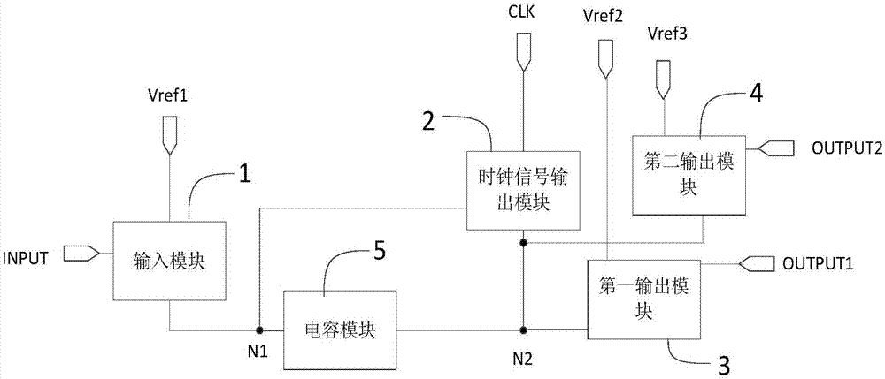
[0099] by figure 1 The circuit configuration shown and Figure 5 The timing diagram shown is illustrated:

[0100] T1 stage, INPUT=1, CLK=0, Vref2=0, Vref3=1.

[0101] Since INPUT=1, the first switch transistor is turned on, and the first reference signal sent by the first reference signal segment is provided to the first node through the turned-on first switch transistor, so that the first node maintains a high potential.

[0102] In T2 stage, INPUT=0, CLK=1, Vref2=1, Vref3=0.

[0103] Due to the effect of the first capacitor, the potential of the first node remains at a high potential, the second switch transistor is turned on, and the clock signal sent by the clock signal terminal is provided to the second node through the turned-on second switch transistor, because the second reference signal at this time The second reference signal sent by the terminal is a high potential, the third switch transistor is turned on, and the potential of the second node is provided to the...

Embodiment 2

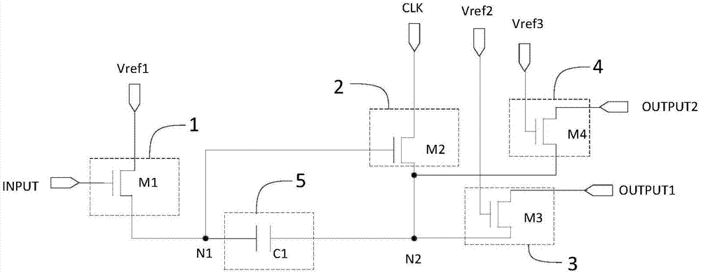
[0105] by figure 1 The circuit configuration shown and Figure 6 The timing diagram shown is illustrated:

[0106] In T1 stage, INPUT=1, CLK=0, Vref2=1, Vref3=0.

[0107] Since INPUT=1, the first switch transistor is turned on, and the first reference signal sent by the first reference signal segment is provided to the first node through the turned-on first switch transistor, so that the first node maintains a high potential.

[0108] In T2 stage, INPUT=0, CLK=1, Vref2=0, Vref3=1.

[0109] Due to the effect of the first capacitor, the potential of the first node remains at a high potential, the second switch transistor is turned on, and the clock signal sent by the clock signal terminal is provided to the second node through the turned-on second switch transistor, because the third reference signal at this time The third reference signal sent by the terminal is a high potential, the fourth switch transistor is turned on, and the potential of the second node is provided to t...


PUM


Abstract

The present invention discloses a shift register, a gate drive circuit and a display device. The shift register comprises an input module, a clock signal output module, a first output module, a second output and a capacitor module. Through arrangement of the first output module and the second output module, the same shift register can output adjacent two rows of gate drive signals in the gate drive circuit and is controlled to perform switching the sequence of output of the gate drive signals of the Nth row of pixels and gate drive signals of the (N+1)th row of pixels to realize row-by-row output or switching output of the gate circuit so as to realize reduction of the polarity hopping of the input data signals and reduce energy consumption.

Description

technical field [0001] The invention relates to the field of display technology, in particular to a shift register, a gate drive circuit and a display device. Background technique [0002] In a flat panel display panel, a gate-on signal is usually provided to gates of thin film transistors (TFT, Thin Film Transistor) in the pixel region through a gate driving circuit. The gate drive circuit can be formed on the array substrate of the flat panel display panel through an array process, that is, the gate driver on array (GOA) process of the array substrate. This integrated process not only saves costs, but also can achieve flat panel display ( At the same time, it also saves the bonding (Bonding) area of ​​the gate integrated circuit (IC, Integrated Circuit) and the wiring space of the fan-out (Fan-out), so that the narrow border design can be realized . [0003] The gate drive circuit is composed of a plurality of cascaded shift registers. The shift registers of each stage a...

Claims


Application Information

Patent Timeline
Patent Type & Authority Applications(China)
IPC IPC(8): G09G3/36G11C19/28
CPCG09G3/3674G09G2310/0286G11C19/28
Inventor 冯博王世君陈希占红明
Owner BOE TECH GRP CO LTD
Why Eureka
Try Eureka