Cross polarization conversion optical device and its design method
A technology of cross polarization and optical devices, applied in the field of optics, can solve the problems of simple structure and high polarization conversion efficiency, and achieve the effect of low cost and high polarization conversion efficiency
- Summary
- Abstract
- Description
- Claims
- Application Information
AI Technical Summary
Problems solved by technology
Method used
Image
Examples
no. 1 example
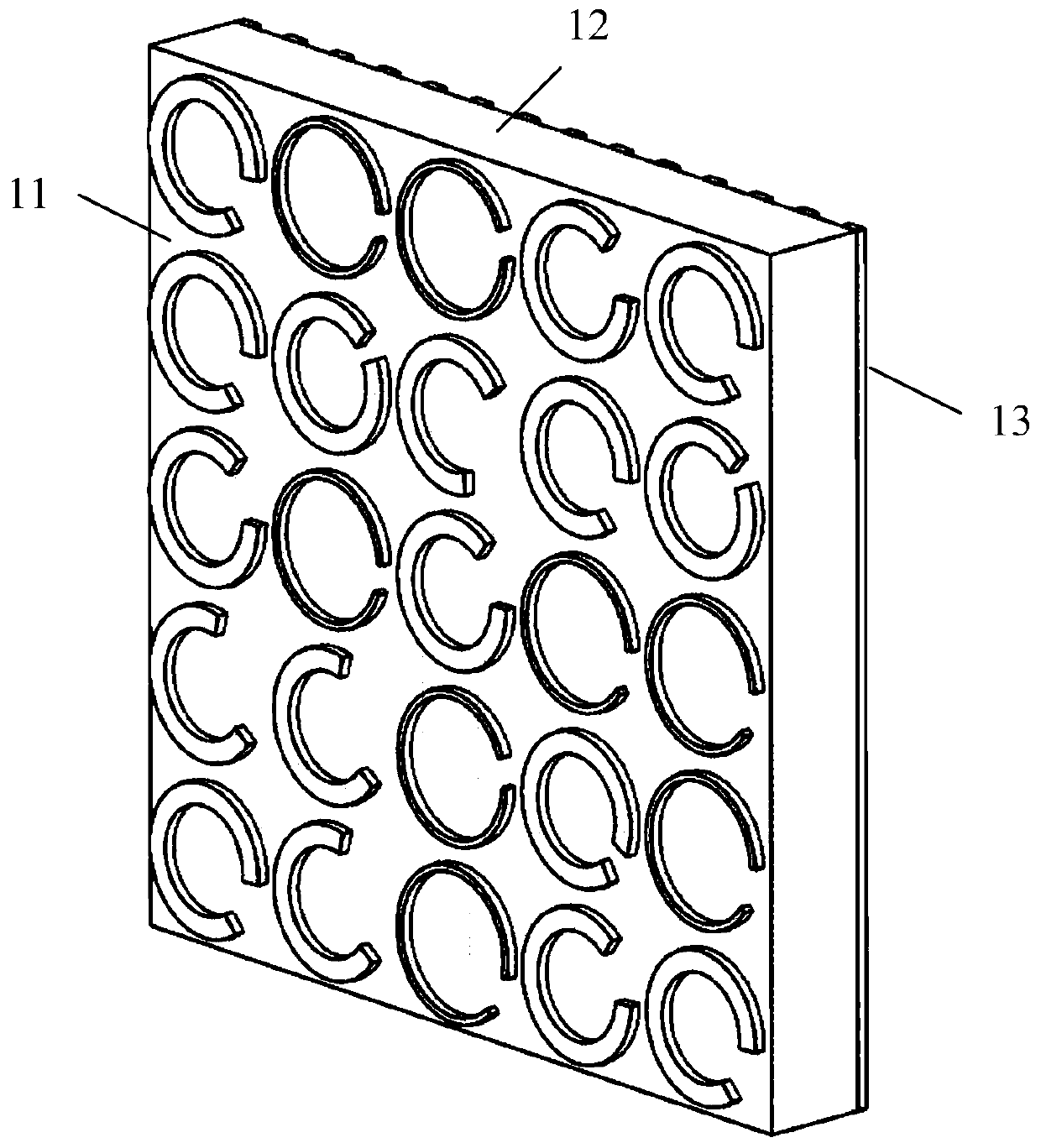
[0055] Such as figure 1 Shown is a partial structural schematic diagram of the cross-polarization conversion optical device according to the first embodiment of the present invention. The cross-polarization conversion optical device has a double-layer metasurface structure, which can be used to achieve full-band beam shaping effects. Such as figure 1 As shown in , the cross polarization conversion optical device is a flat plate structure, including: a "C" structure metal layer 11, a dielectric layer 12 and a metal grating layer 13.
[0056] The "C" structure metal layer 11 can be a good conductor, such as gold, silver, copper, aluminum and other precious metals. The "C" structure metal layer 11 includes a plurality of "C" structural units, and the multiple "C" structural units array arrangement.
[0057] In the first embodiment of the present invention, the "C" structure metal layer 11 is made of gold, and the "C" structure metal layer 11 contains 128*128 "C" structure unit...
no. 2 example
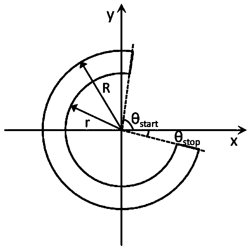
[0074] The design method of the cross-polarization conversion optical device according to the second embodiment of the present invention modulates the excitation of the light beam incident on the cross-polarization conversion optical device by modulating the outer radius, inner radius, start angle and end angle of the "C" structural unit. Amplitude and phase of a radiated field with a vertical polarization state.
[0075] Figure 6 It is a flow chart of the design method of the cross polarization conversion optical device according to the second embodiment of the present invention, and the design method specifically includes the following steps:
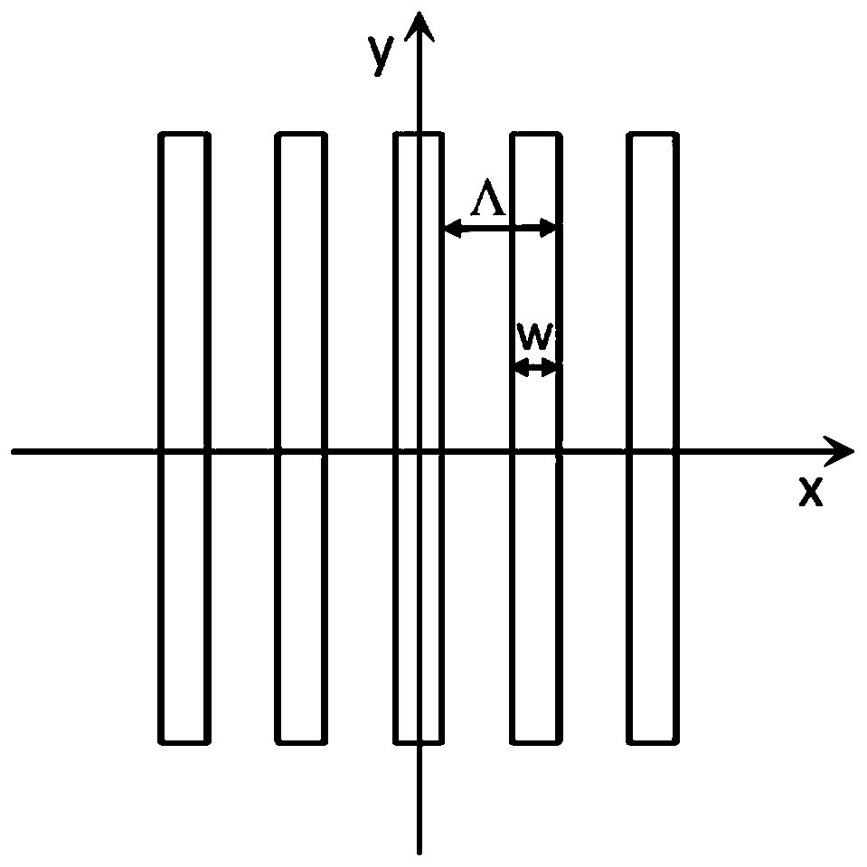
[0076] 601. Calculate the grating period and the grating width of the metal grating layer. Specifically, the parameters of the dielectric layer and the "C" structure metal layer are kept constant, and the grating period and grating width of the metal grating layer are calculated according to the Fappaut resonance theory.
[0077] I...
no. 3 example
[0102] Steps 701 to 704 are the same as steps 601 to 604 in the second embodiment of the present invention.
[0103] 705 , using a group of "C" structural units obtained in step 704 to design a two-dimensional array of "C" structural metal layers. Specifically, the photoinduced results, the shape and size of the two-dimensional array are set, and the optimal arrangement of the two-dimensional array composed of eight "C" structural units is calculated.
[0104] In the third embodiment of the present invention, it is set that after the incident light of x polarization passes through the cross-polarization conversion optical device with the two-dimensional array of metal layers with the "C" structure, the optical result of focusing lens converging imaging on the object is realized; setting two The shape of the three-dimensional array is square, the size is 128*128 "C" structural units, and the center-to-center distance between two adjacent "C" structural units is 80 μm.
[0105]...
PUM
 Abstract
Description
Claims
Application Information
 - R&D Engineer
- R&D Manager
- IP Professional
- Industry Leading Data Capabilities
- Powerful AI technology
- Patent DNA Extraction
Browse by: Latest US Patents, China's latest patents, Technical Efficacy Thesaurus, Application Domain, Technology Topic, Popular Technical Reports.
© 2024 PatSnap. All rights reserved.Legal|Privacy policy|Modern Slavery Act Transparency Statement|Sitemap|About US| Contact US: help@patsnap.com


