
Optical module structure

A technology of optical module and connection structure, which is applied in the field of optical communication, can solve problems such as poor signal transmission performance and interconnection impedance mismatch, and achieve the effects of reducing loss, shortening interconnection, and increasing transmission rate

Active Publication Date: 2017-12-15
NAT CENT FOR ADVANCED PACKAGING
View PDF3 Cites 5 Cited by
  • Summary
  • Abstract
  • Description
  • Claims
  • Application Information

AI Technical Summary

Problems solved by technology

[0004] Therefore, the technical problem to be solved by the present invention is to overcome the defect of poor signal transmission performance caused by the interconnection impedance mismatch between the optical chip and the electrical chip in the prior art

Method used


Image

  • Optical module structure
  • Optical module structure
  • Optical module structure

Examples


Embodiment Construction

[0040] The technical solutions of the present invention will be clearly and completely described below in conjunction with the accompanying drawings. Apparently, the described embodiments are some of the embodiments of the present invention, but not all of them. Based on the embodiments of the present invention, all other embodiments obtained by persons of ordinary skill in the art without making creative efforts belong to the protection scope of the present invention.

[0041] In the description of the present invention, it should be noted that the terms "center", "upper", "lower", "left", "right", "vertical", "horizontal", "inner", "outer" etc. The indicated orientation or positional relationship is based on the orientation or positional relationship shown in the drawings, and is only for the convenience of describing the present invention and simplifying the description, rather than indicating or implying that the referred device or element must have a specific orientation, ...


PUM


Abstract

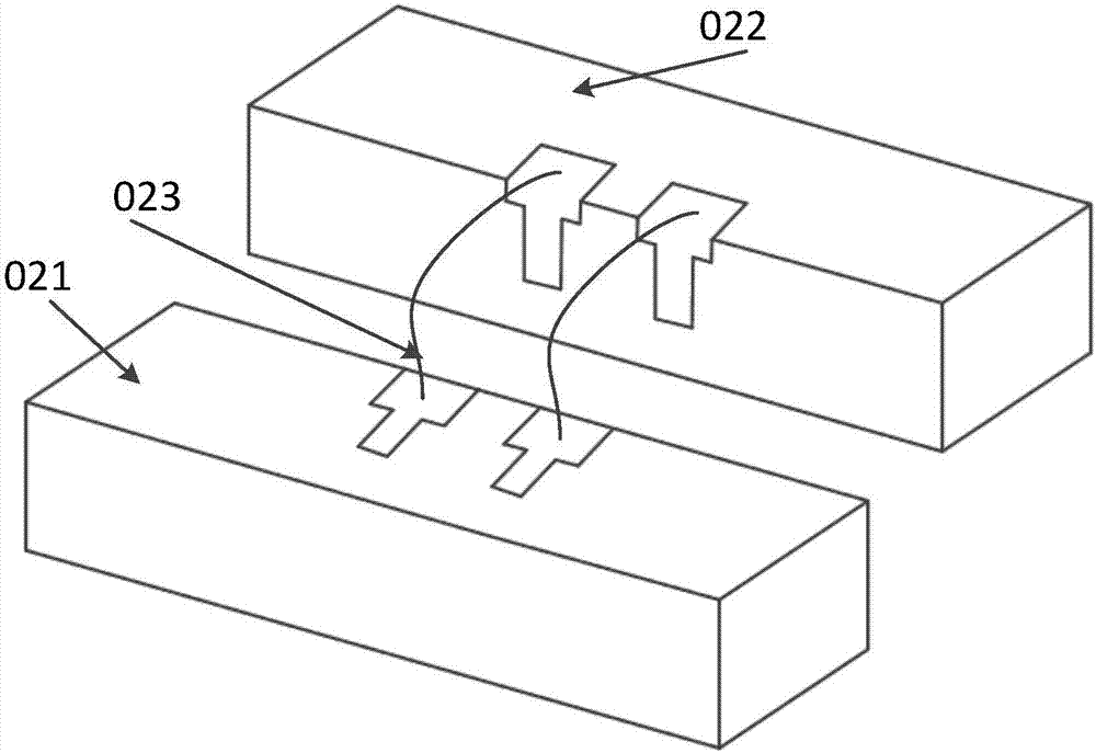
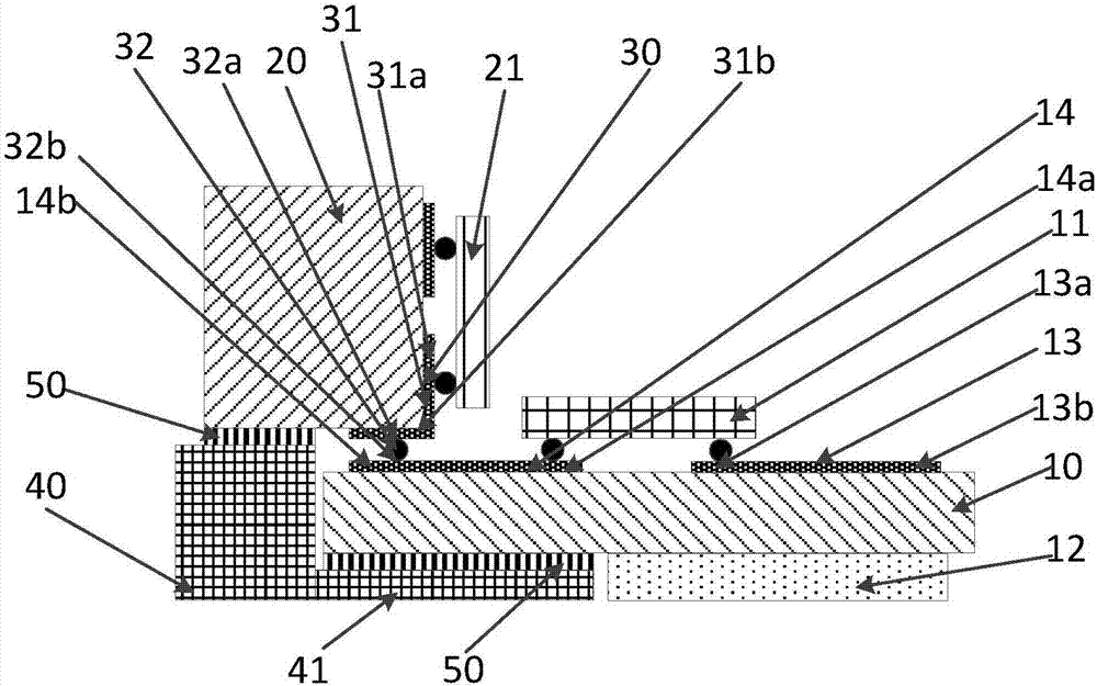
The present invention provides an optical module structure. The optical module structure comprises a first carrying plate and a second carrying plate; the upper surface of the first carrying plate is provide with an electric chip; the second carrying plate is disposed above the first carrying plate; a side wall of the second carrying plate, which is adjacent to the electric chip, is provided with a photoelectric conversion element; and the photoelectric conversion element is connected with the electric chip through a connection structure. According to the optical module structure of the invention, the photoelectric conversion element is disposed above the electric chip, and therefore, by means of such a flip-chip bonding mode, connection between the photoelectric conversion element and the electric chip can be shortened, loss can be reduced, and a transmission rate can be increased.

Description

technical field [0001] The invention relates to the technical field of optical communication, in particular to an optical module structure. Background technique [0002] With the rapid development of integrated circuits, chip processing capabilities are getting stronger and stronger, and the requirements for transmission rate and transmission capacity are also getting higher and higher. Optical interconnection technology has the advantages of high bandwidth, low delay, and light weight, so it has a wide range of market demands and application prospects. At present, with the rapid development of big data and cloud computing, it is necessary to realize the storage and exchange of massive data, and the short-distance optical interconnection transmission scheme applied between servers or between servers and routers has emerged as the times require. The key to this interconnection technology is the fabrication of photoelectric conversion modules with small size, low power consum...

Claims


Application Information

Patent Timeline
Patent Type & Authority Applications(China)
IPC IPC(8): G02B6/42
CPCG02B6/4274
Inventor 薛海韵何慧敏曹立强
Owner NAT CENT FOR ADVANCED PACKAGING
Learn More