A kind of preparation method of inorganic quantum dot light-emitting diode device
A quantum dot light-emitting and diode technology, which is applied in semiconductor/solid-state device manufacturing, semiconductor devices, electric solid-state devices, etc., can solve problems such as difficult injection of electrons and holes into the light-emitting layer, low exciton recombination efficiency, and high operating voltage of devices , to achieve the effects of low preparation difficulty, good charge injection and transport capabilities, and stable device performance
- Summary
- Abstract
- Description
- Claims
- Application Information
AI Technical Summary
Problems solved by technology
Method used
Image
Examples
Embodiment 1
[0028] A preparation of an inorganic quantum dot light-emitting diode device, the preparation steps of the method are as follows:
[0029] Step 1: Rinse the ITO transparent conductive glass substrate in deionized water first, then wash it repeatedly with deionized water, acetone, and ethanol three times, and bake it in a clean environment until the water is completely removed;
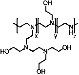
[0030] The second step: PEIE is diluted with ethanol to a concentration of 0.1 wt%, and then coated with PEIE solution on the ITO transparent conductive glass substrate to form a PEIE film layer of about 10 nm;
[0031] The third step: PEIE was mixed into the ZnO nanoparticle solution with a doping concentration of 0.1 wt%, and then the mixed solution of ZnO:PEIE was coated on the substrate to form a ZnO:PEIE film layer with a thickness of 60 nm, wherein ZnO The nanoparticle solution is prepared by a common process, which is prepared by the mixed reaction of zinc acetate and tetramethylammonium hydroxi...
Embodiment 2
[0035] The difference between Example 2 and Example 1 is that the concentration of the ethanol solution in the second step is 0.05 wt%, and a PEIE film layer of about 5 nm is formed.
Embodiment 3
[0037] The difference between Example 3 and Example 1 is that the concentration of the mixed solution of ZnO:PEIE in the third step is 0.05 wt%, and the thickness of the film layer is 50 nm.
PUM
| Property | Measurement | Unit |
|---|---|---|
| thickness | aaaaa | aaaaa |
| diameter | aaaaa | aaaaa |
| thickness | aaaaa | aaaaa |
Abstract
Description
Claims
Application Information
 - R&D
- Intellectual Property
- Life Sciences
- Materials
- Tech Scout
- Unparalleled Data Quality
- Higher Quality Content
- 60% Fewer Hallucinations
Browse by: Latest US Patents, China's latest patents, Technical Efficacy Thesaurus, Application Domain, Technology Topic, Popular Technical Reports.
© 2025 PatSnap. All rights reserved.Legal|Privacy policy|Modern Slavery Act Transparency Statement|Sitemap|About US| Contact US: help@patsnap.com


