


Quick Research
Generate reliable direction feasibility study reports for your R&D in just a few steps.

Technical Q&A
Discover and master advanced knowledge NOW. Basics, ideas, possibilities, all at once.

Find Solutions
As an expert in R&D theories, this can generate solutions to your technical problems instantly.

Evaluate Feasibility
Analyze your overall solution with one click, know your potential R&D risks in advance.

Monitor Landscape
Get weekly tech updates, stay abreast of the latest tech innovations and key insights.
Preparation method of vertical-structure SnSe2/MoSe2 novel heterojunctions and method for modifying field effect properties thereof
A vertical structure and heterojunction technology, which is applied in semiconductor/solid-state device manufacturing, electrical components, circuits, etc., can solve the problems of complex vertical structure heterojunction, expensive experimental equipment, toxicity, etc., and achieve low equipment cost and abundant energy. With engineering, the effect that the operation method is simple
- Summary
- Abstract
- Description
- Claims
- Application Information
AI Technical Summary
Problems solved by technology
Method used
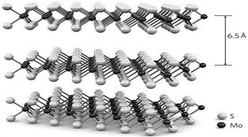
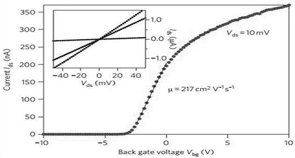
Image

Examples
Embodiment Construction
[0027] The present invention will be further described below in conjunction with specific embodiments. It should be understood that the following examples are only used to illustrate the present invention rather than limit the scope of the present invention, and those skilled in the art can make some non-essential improvements and adjustments based on the content of the above invention.
[0028] The SnSe with vertical structure of this embodiment 2 / MoSe 2 The preparation method of the novel heterojunction is as follows:
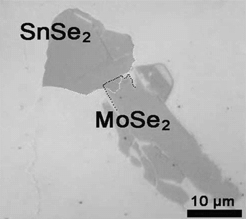
[0029] (1) From SnSe by mechanical exfoliation 2 Bulk materials get few-layer SnSe 2 Nanomaterials, transferred to SiO 2 / Si substrate, prepared few-layer SnSe 2 / SiO 2 / Si nanomaterials; from MoSe by mechanical exfoliation 2 Bulk materials get few-layer MoSe 2 Nanomaterials, transferred onto Si substrates, to produce few-layer MoSe 2 / Si nanomaterials;
[0030] (2) The few-layer SnSe prepared in step (1) 2 / SiO 2 / Si nanomaterials are placed o...
PUM
 Abstract
Description
Claims
Application Information
 - R&D Engineer
- R&D Manager
- IP Professional
- Industry Leading Data Capabilities
- Powerful AI technology
- Patent DNA Extraction
Browse by: Latest US Patents, China's latest patents, Technical Efficacy Thesaurus, Application Domain, Technology Topic, Popular Technical Reports.
© 2024 PatSnap. All rights reserved.Legal|Privacy policy|Modern Slavery Act Transparency Statement|Sitemap|About US| Contact US: help@patsnap.com