
Full coverage type one-time smooth electrode light emitting diode and manufacturing method thereof

A light-emitting diode, full-coverage technology, applied to circuits, electrical components, semiconductor devices, etc., can solve problems such as poor adhesion of metal layers, inability to carry out large-scale mass production, and affect product quality and yield, so as to reduce pollution and solution contact denaturation, avoiding electrode edge shedding, improving quality and reliability

Inactive Publication Date: 2017-10-13
YANGZHOU CHANGELIGHT
View PDF2 Cites 0 Cited by
  • Summary
  • Abstract
  • Description
  • Claims
  • Application Information

AI Technical Summary

Problems solved by technology

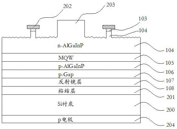
[0004] Due to the dense and smooth surface of the n-GaAs contact layer, poor adhesion to the metal layer, and the n-GaAs contact layer material itself is prone to denaturation when exposed to chemical solutions, wet etching of the n-GaAs contact layer and n-AIGaInP rough When the layer is formed, there is side etching, so that the edge of the n extended electrode 202 is in a suspended state (from figure 1 Visible), the adverse consequences are: in the follow-up operation process, under the action of external stress and solution penetration, it is easy to cause the expansion electrode and n-GaAs contact layer to be damaged and fall off, affecting the normal ohmic contact and

Method used


Image

  • Full coverage type one-time smooth electrode light emitting diode and manufacturing method thereof
  • Full coverage type one-time smooth electrode light emitting diode and manufacturing method thereof
  • Full coverage type one-time smooth electrode light emitting diode and manufacturing method thereof

Examples


Example Embodiment

[0026] 1. Manufacturing process:

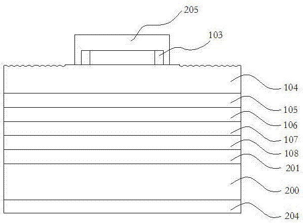
[0027] 1. Preparation of the light-emitting diode epitaxial wafer: on one side of a temporary GaAs substrate 100, the buffer layer 101, the barrier layer 102, the n-GaAs ohmic contact layer 103, and n-AIGaInP are used to epitaxially grow the buffer layer 101, the barrier layer 102, and the n-AIGaInP in sequence. Layer 104, MQW multiple quantum well active layer 105, p-AIGaInP confinement layer 106, and p-GaP window layer 107.

[0028] The mirror layer 108 is vapor-deposited on the p-GaP window layer 107, and SiO 2 Evaporate, in SiO 2 Conductive small holes are opened on the layer, and then Ag is evaporated.

[0029] The mirror layer 108 also functions to form an ohmic contact with the p-GaP window layer 107. Among them, it uses SiO with conductive small holes 2 The layer can adjust the number, distribution, aperture, and spacing of small holes according to actual needs, so as to adjust the conductive effect and reflection effect of the chip, so as ...


PUM


Abstract

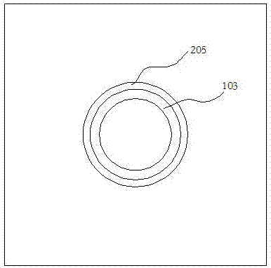
The invention discloses a full coverage type one-time smooth electrode light emitting diode and a manufacturing method thereof and belongs to the technical field of semiconductor devices. After a temporary substrate, a buffer layer and a barrier layer in a bonded semi-finished product are completely removed, a full coverage n electrode layer is manufactured through evaporation on a graphical n-GaAs ohmic contact layer, so that the n electrode covers the graphical n-GaAs ohmic contact layer. An ohmic contact extension electrode and a main electrode are formed at one time, the n electrode layer obtained through one-time evaporation covers the extension electrode and the main electrode which form the ohmic contact with the graphical n-GaAs ohmic contact layer, so that the problems that coarsening is non-uniform to cause abnormal electrode appearance identification and a coarsening stage is too large to make the thickness of an evaporation metal layer unable to be effectively filled in order to have the rupture phenomenon and finally cause the shedding phenomenon of the electrode edge are avoided.

Description

technical field [0001] The invention belongs to the technical field of semiconductor devices, in particular to the technical field of light-emitting diode manufacture. Background technique [0002] The main markets for high-brightness AlGaInP light-emitting diodes include monochrome display subtitles for road conditions and highway information; full-color billboards for large display screens; light-emitting diodes for automotive interior and exterior lighting; backlights for portable products; architectural and special Lighting applications for lighting; and applications in electronic equipment, as industrial indicator lights and indicator lights according to customer requirements. The AlGaInP material can adjust the molar composition of Al to make the bandgap width and the GaAs substrate have a good lattice match, but it has serious absorption of red and yellow light, and due to the AlGaInP-GaAs semiconductor refractive index, for smooth On the surface, only a small part o...

Claims


Application Information

Patent Timeline
IPC IPC(8): H01L33/38H01L33/00
CPCH01L33/0093H01L33/38H01L2933/0016
Inventor 陈宝马祥柱杨凯李全素
Owner YANGZHOU CHANGELIGHT
Learn More