
NBTI degradation model obtaining method based on nonuniform distribution interface traps

A technology of non-uniform distribution and interface traps, which is applied in the fields of instrumentation, calculation, electrical and digital data processing, etc., can solve the problems of accurate calculation of the distribution of interface traps in the channel edge region, and achieves wide applicability, few fitting parameters, and reliable devices. Sexually accurate effects

Active Publication Date: 2017-09-29
EAST CHINA NORMAL UNIV +1
View PDF2 Cites 4 Cited by
  • Summary
  • Abstract
  • Description
  • Claims
  • Application Information

AI Technical Summary

Problems solved by technology

[0004] Since the existing NBTI degradation model does not have an accurate calculation of the distribution of interface traps in the channel edge region, in order to obtain a more accurate degradation model formula, the present invention proposes a method that considers the influence of device channel length and width geometry, based on The NBTI degradation model acquisition method of non-uniformly distributed interface traps, the model obtained by this method has high physical significance, and has certain scalability and universality

Method used


Image

  • NBTI degradation model obtaining method based on nonuniform distribution interface traps
  • NBTI degradation model obtaining method based on nonuniform distribution interface traps
  • NBTI degradation model obtaining method based on nonuniform distribution interface traps

Examples


Embodiment Construction

[0042] The present invention will be further described in detail in conjunction with the following specific embodiments and accompanying drawings. The process, conditions, experimental methods, etc. for implementing the present invention, except for the content specifically mentioned below, are common knowledge and common knowledge in this field, and the present invention has no special limitation content.

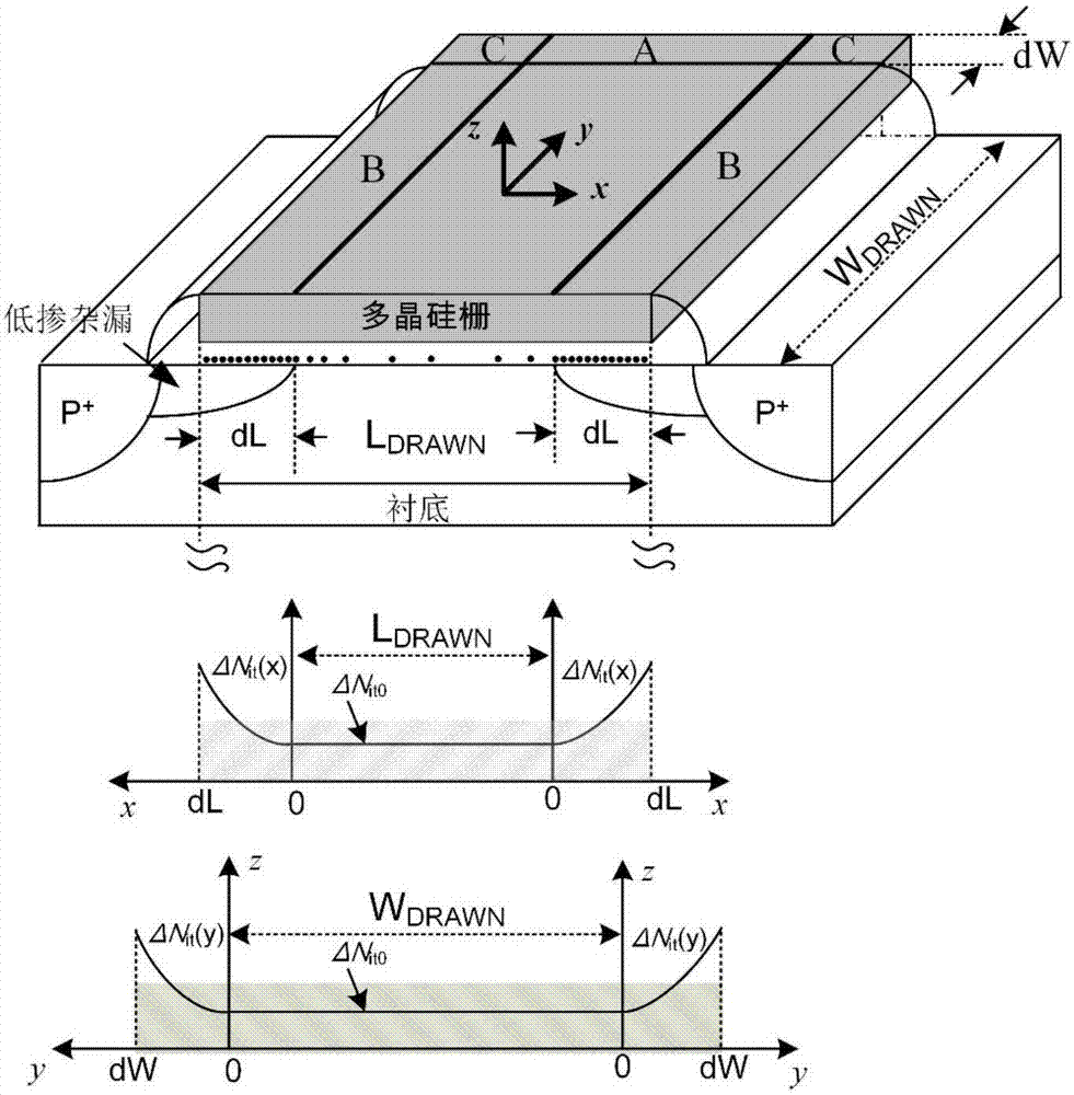
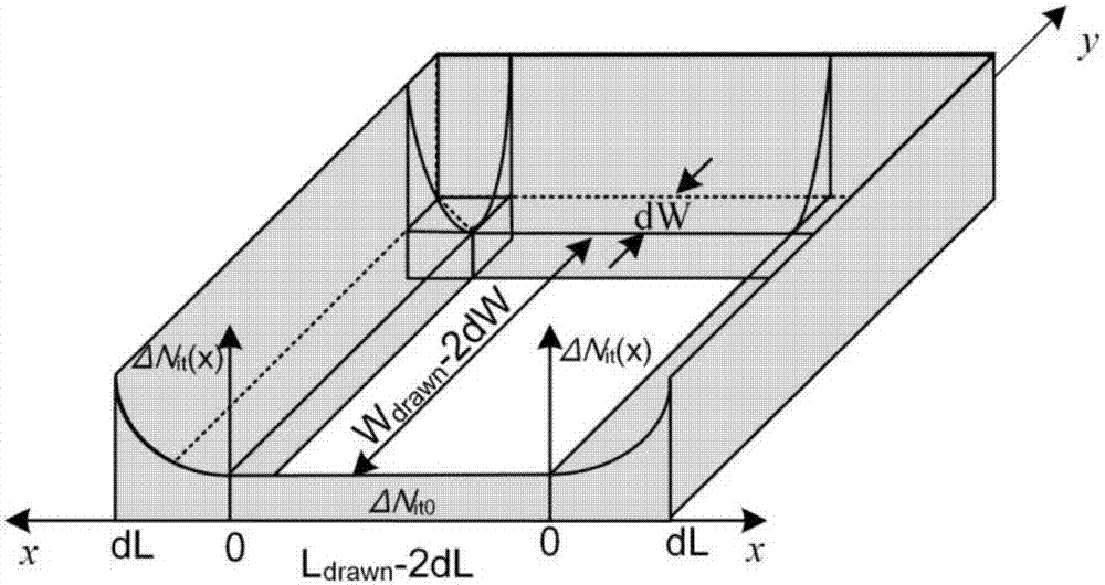
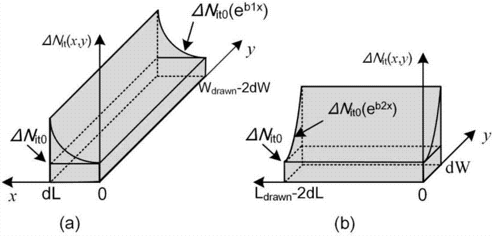
[0043] The NBTI degradation model provided by the present invention is based on the non-uniform distribution of interface traps, taking into account the influence of device geometry channel length and width, and accurately calculates the distribution frame and total density of interface traps. The modeling process of the present invention includes the following steps:

[0044] Step 1: Divide the interface trap ΔN in different regions of the MOS device IT distributed

[0045] according to figure 1 The schematic diagram of the distribution division of ΔNit is shown, and t...


PUM


Abstract

The invention discloses an NBTI degradation model obtaining method based on nonuniform distribution interface traps. The method comprises the steps that 1, interface trap distributions in different zone of an MOS device are divided to obtain total distribution frame of the interface traps; 2, according to geometric construction, the interface trap distribution density in each zone is calculated, and the total density of the nonuniform distribution interface traps is obtained; 3, threshold voltage deviation caused by NBTI is obtained according to the deltaNIT total density, and an NBTI degradation model based on geometric construction analysis is obtained. The actual distribution situation of the interface traps produced by an NBTI effect is incorporated in the model, accordingly the total density of interface trap charges produced in the MOS device can be accurately calculated, thus a threshold voltage degradation model is obtained, few fitting parameters are required, the applicability is wide, and the model provides more accurate precision for device reliability.

Description

technical field [0001] The invention belongs to the technical field of semiconductors, in particular to an accurate acquisition method of an NBTI degradation model based on non-uniformly distributed interface traps. Background technique [0002] As semiconductor process technology enters the deep submicron era, negative bias temperature instability (NBTI) has become one of the main factors affecting device performance degradation and lifespan. A model that accurately describes the physical mechanism and performance of device degradation is an important aspect of device reliability. A big problem that needs to be solved and perfected urgently. It has been proposed that the interface traps caused by negative bias temperature instability are not uniformly distributed in the channel, and the NBTI degradation strongly depends on the device geometry, especially the length and width of the channel. But so far this aspect has received little attention. The generally accepted react...

Claims


Application Information

Patent Timeline
Patent Type & Authority Applications(China)
IPC IPC(8): G06F19/00
CPCG16Z99/00
Inventor 李小进曾严孙亚宾石艳玲胡少坚郭奥田明廖端泉王昌锋
Owner EAST CHINA NORMAL UNIV
Learn More