A Method for Obtaining Parasitic Capacitance Models Around the Gate of 3D MOS Devices

A MOS device and parasitic capacitance technology, which is applied in the field of accurate model acquisition of the parasitic capacitance around the gate of a three-dimensional MOS device, can solve problems such as slow calculation speed, difficulty in establishing capacitance models, and inability to obtain accurate continuous capacitance models, and achieves fewer fitting parameters. , the effect of wide applicability

Active Publication Date: 2019-05-17
EAST CHINA NORMAL UNIV
View PDF3 Cites 0 Cited by
  • Summary
  • Abstract
  • Description
  • Claims
  • Application Information

AI Technical Summary

Problems solved by technology

The first method can only calculate accurate discrete capacitance data of a specific structure according to fixed conditions, but the calculation speed is slow, and it is impossible to obtain an accurate and continuous capacitance model with physical meaning and universal applicability, nor can it provide designers with accurate capacitance data. Analysis reference
The problem with the second method is that it is difficult to obtain a cell structure capacitance model based on physical meaning and simple formula, especially in the case of multiple materials, it is difficult to establish a capacitance model

Method used


Image

  • A Method for Obtaining Parasitic Capacitance Models Around the Gate of 3D MOS Devices
  • A Method for Obtaining Parasitic Capacitance Models Around the Gate of 3D MOS Devices
  • A Method for Obtaining Parasitic Capacitance Models Around the Gate of 3D MOS Devices

Examples


Embodiment Construction

[0041] The present invention will be further described in detail in conjunction with the following specific embodiments and accompanying drawings. The process, conditions, experimental methods, etc. for implementing the present invention, except for the content specifically mentioned below, are common knowledge and common knowledge in this field, and the present invention has no special limitation content.

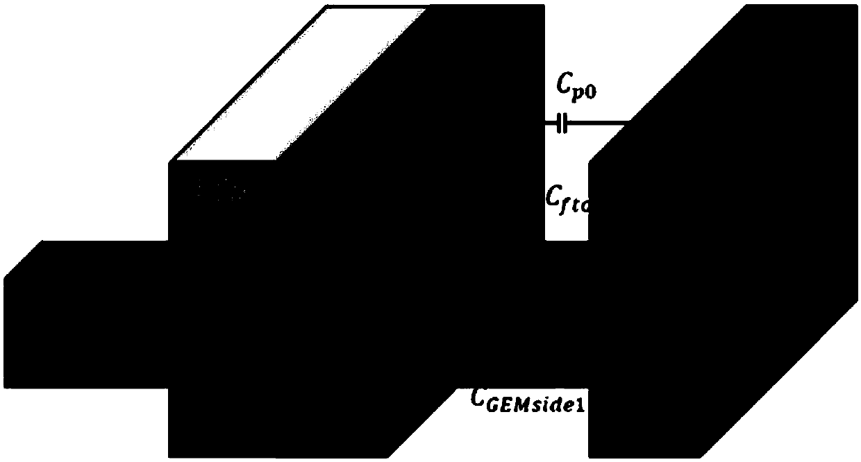
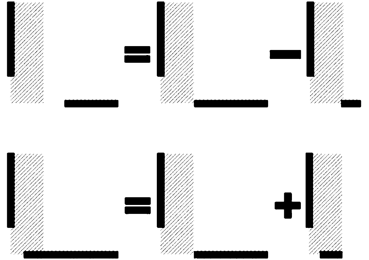
[0042] The parasitic capacitance model around the gate of the three-dimensional MOS device provided by the invention is based on the conformal transformation and can solve the situation of including multiple dielectric layers. The modeling process of the present invention includes the following steps:

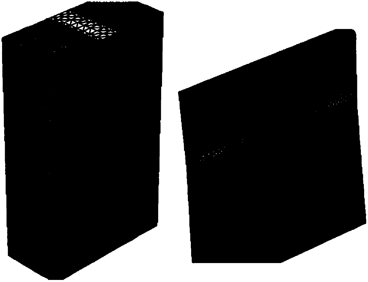
[0043] Step 1: Method for dividing the parasitic capacitance around the gate of the three-dimensional MOS device. The reference basic parameters of the three-dimensional MOS device in the present invention are shown in Table 1.

[0044] Table 1: Basic parameters of three-...


PUM


Abstract

The invention discloses a method for acquiring a gate fringe parasitic capacitance model of a three-dimensional MOS device. The method comprises the steps of 1: dividing gate fringe parasitic capacitance of the three-dimensional MOS device to obtain a basic capacitance structure model containing parallel plate capacitance and perpendicular plate capacitance; 2: approximately calculating unit capacitance of the basic capacitance structure model; 3: deducing a multi-media perpendicular plate capacitance model based on conformal mapping; and 4: extracting a correction factor of the multi-media perpendicular plate capacitance model, and correcting the multi-media perpendicular plate capacitance model according to the correction factor so as to obtain the gate fringe parasitic capacitance model of the three-dimensional MOS device. The model proposed in the method is incorporated into an actual situation of a multimedia material, so that the gate fringe parasitic capacitance of the three-dimensional MOS device can be accurately calculated; and according to the method, few fitting parameters are required and the applicability is wide.

Description

technical field [0001] The invention belongs to the technical field of semiconductors, in particular to a method for obtaining an accurate model of parasitic capacitance around a gate of a three-dimensional MOS device. Background technique [0002] With the gradual reduction of the feature size of the semiconductor integrated circuit process to the nanometer field, the three-dimensional MOS device has gradually become the mainstream core device, and a complete set of models that accurately describe the working state and performance of the device is a major problem that needs to be solved and improved urgently. Among them, the parasitic capacitance around the Fin structure is difficult to accurately model because of its three-dimensional structure and filling with various materials. Therefore, the accurate model of the parasitic capacitance of the three-dimensional MOS device is a difficult point in the complete set of device models, and it is also a key link in analyzing the...

Claims


Application Information

Patent Timeline
Patent Type & Authority Patents(China)
IPC IPC(8): G06F17/50
CPCG06F30/367
Inventor 郑芳林孙立杰任佳琪刘程晟石艳玲李小进孙亚宾
Owner EAST CHINA NORMAL UNIV
Why Eureka
Try Eureka