


Quick Research
Generate reliable direction feasibility study reports for your R&D in just a few steps.

Technical Q&A
Discover and master advanced knowledge NOW. Basics, ideas, possibilities, all at once.

Find Solutions
As an expert in R&D theories, this can generate solutions to your technical problems instantly.

Evaluate Feasibility
Analyze your overall solution with one click, know your potential R&D risks in advance.

Monitor Landscape
Get weekly tech updates, stay abreast of the latest tech innovations and key insights.
One-bit full-adder based on FinFET transistors
A full adder and transistor technology, applied in the field of a full adder, to achieve the effect of reducing power consumption and the number of tubes
- Summary
- Abstract
- Description
- Claims
- Application Information
AI Technical Summary
Problems solved by technology
Method used
Image

Examples
Embodiment 1
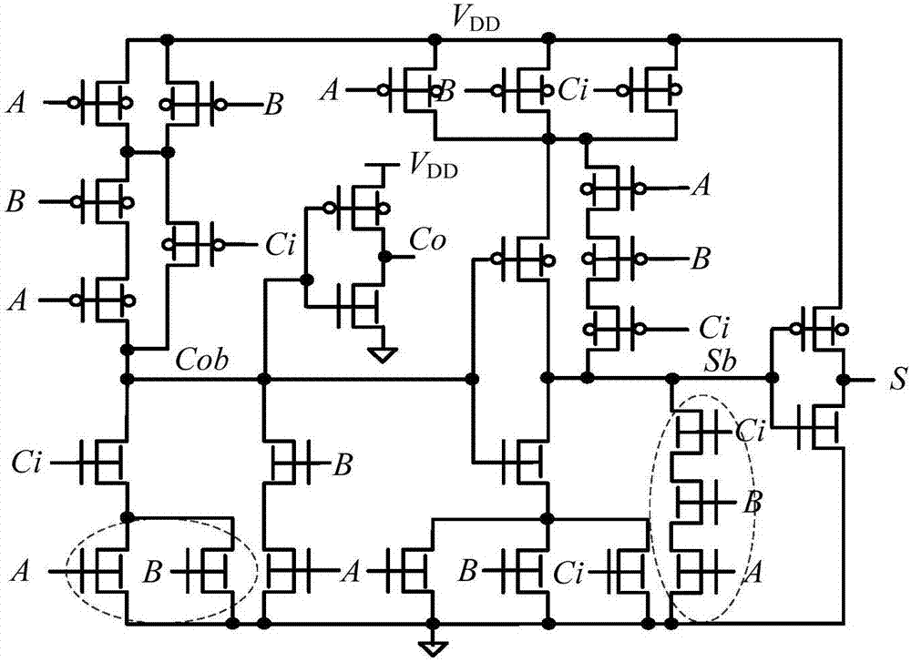
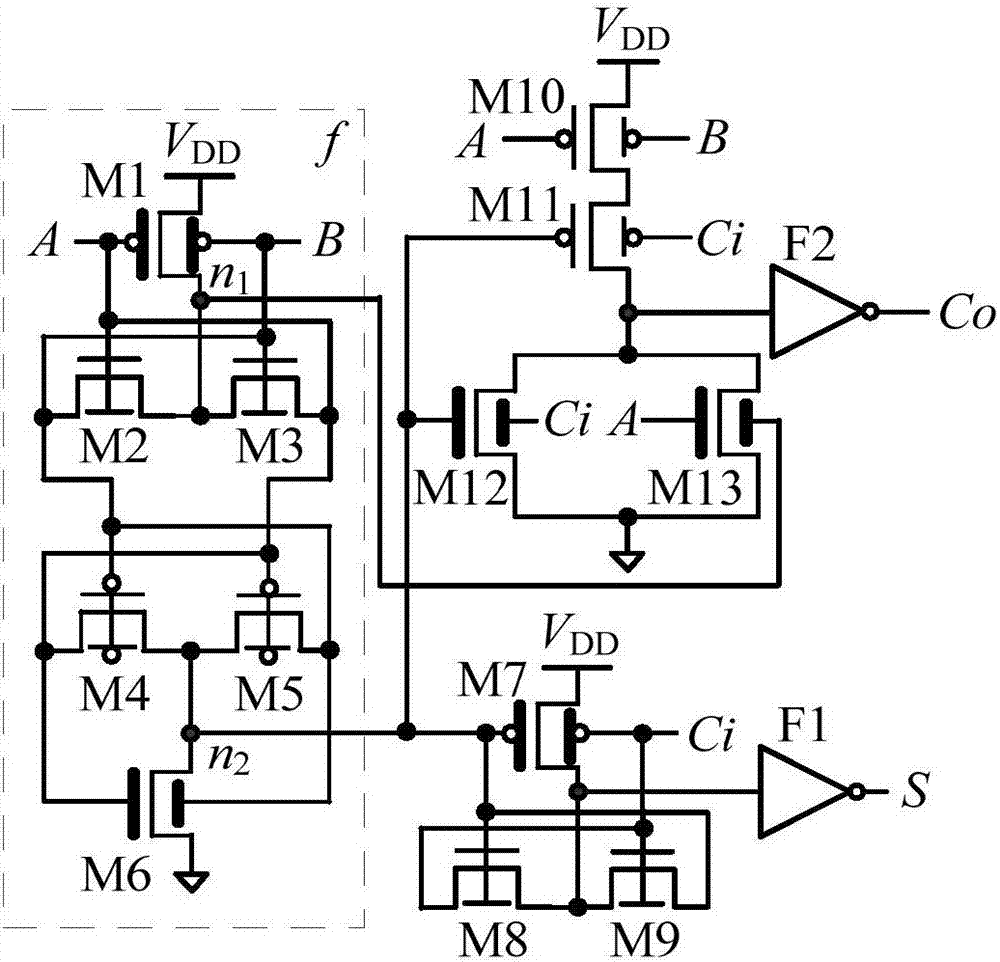
[0021] Embodiment one: if image 3 As shown, a one-bit full adder based on FinFET transistors includes a first FinFET tube M1, a second FinFET tube M2, a third FinFET tube M3, a fourth FinFET tube M4, a fifth FinFET tube M5, and a sixth FinFET tube M6, the seventh FinFET tube M7, the eighth FinFET tube M8, the ninth FinFET tube M9, the tenth FinFET tube M10, the eleventh FinFET tube M11, the twelfth FinFET tube M12, the thirteenth FinFET tube M13, the first The phase device F1 and the second inverter F2, the first FinFET tube M1, the fourth FinFET tube M4, the fifth FinFET tube M5, the seventh FinFET tube M7, the tenth FinFET tube M10 and the eleventh FinFET tube M11 are all P type FinFET tube, the second FinFET tube M2, the third FinFET tube M3, the sixth FinFET tube M6, the eighth FinFET tube M8, the ninth FinFET tube M9, the twelfth FinFET tube M12 and the thirteenth FinFET tube M13 are all N FinFET tubes, the first FinFET tube M1, the sixth FinFET tube M6, the seventh Fin...
Embodiment 2
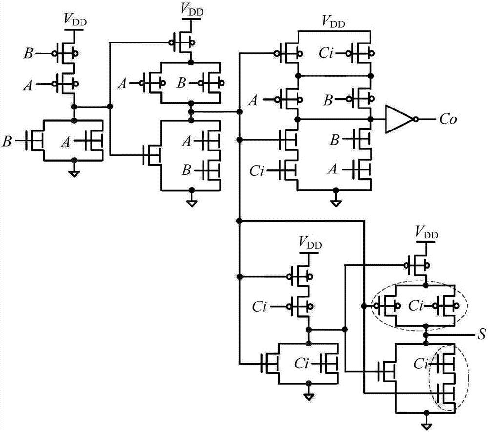
[0022] Embodiment two: if image 3As shown, a one-bit full adder based on FinFET transistors includes a first FinFET tube M1, a second FinFET tube M2, a third FinFET tube M3, a fourth FinFET tube M4, a fifth FinFET tube M5, and a sixth FinFET tube M6, the seventh FinFET tube M7, the eighth FinFET tube M8, the ninth FinFET tube M9, the tenth FinFET tube M10, the eleventh FinFET tube M11, the twelfth FinFET tube M12, the thirteenth FinFET tube M13, the first The phase device F1 and the second inverter F2, the first FinFET tube M1, the fourth FinFET tube M4, the fifth FinFET tube M5, the seventh FinFET tube M7, the tenth FinFET tube M10 and the eleventh FinFET tube M11 are all P type FinFET tube, the second FinFET tube M2, the third FinFET tube M3, the sixth FinFET tube M6, the eighth FinFET tube M8, the ninth FinFET tube M9, the twelfth FinFET tube M12 and the thirteenth FinFET tube M13 are all N FinFET tubes, the first FinFET tube M1, the sixth FinFET tube M6, the seventh FinF...
PUM
 Abstract
Description
Claims
Application Information
 - R&D Engineer
- R&D Manager
- IP Professional
- Industry Leading Data Capabilities
- Powerful AI technology
- Patent DNA Extraction
Browse by: Latest US Patents, China's latest patents, Technical Efficacy Thesaurus, Application Domain, Technology Topic, Popular Technical Reports.
© 2024 PatSnap. All rights reserved.Legal|Privacy policy|Modern Slavery Act Transparency Statement|Sitemap|About US| Contact US: help@patsnap.com