
Ultrasonic sensor and manufacturing method thereof

An ultrasonic sensor technology, applied in the field of ultrasonic sensor and its manufacturing, can solve the problems of complicated manufacturing process, increased manufacturing cost, lower yield rate, etc., and achieve the effect of improving scanning recognition speed, reducing manufacturing cost, and improving yield

Inactive Publication Date: 2017-09-26
HANGZHOU SILAN MICROELECTRONICS
View PDF14 Cites 19 Cited by
  • Summary
  • Abstract
  • Description
  • Claims
  • Application Information

AI Technical Summary

Problems solved by technology

However, during the bonding process, the bonding paste overflow phenomenon will occur, which will cause the structural components of the die to short-circuit and fail, greatly reducing the yield
At the same time, the alignment accuracy of the bonding process is not high, resulting in a large size of the eutectic bonding point for the electrical connection between the two wafers, which increases the manufacturing cost
Integrating CMOS circuits and ultrasonic transducers using a bonding process leads to complex manufacturing processes, high costs and low yields

Method used


Image

  • Ultrasonic sensor and manufacturing method thereof
  • Ultrasonic sensor and manufacturing method thereof
  • Ultrasonic sensor and manufacturing method thereof

Examples


Embodiment Construction

[0060] Hereinafter, the present invention will be described in more detail with reference to the accompanying drawings. In the various figures, identical elements are indicated with similar reference numerals. For the sake of clarity, various parts in the drawings have not been drawn to scale. Also, some well-known parts may not be shown.

[0061] In the following, many specific details of the present invention are described, such as device structures, materials, dimensions, processing techniques and techniques, for a clearer understanding of the present invention. However, the invention may be practiced without these specific details, as will be understood by those skilled in the art.

[0062] The invention can be embodied in various forms, some examples of which are described below.

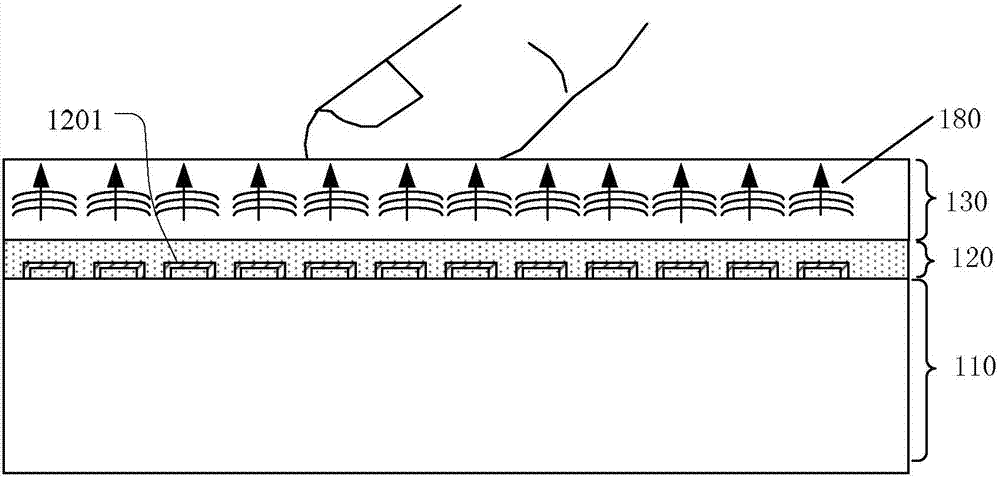
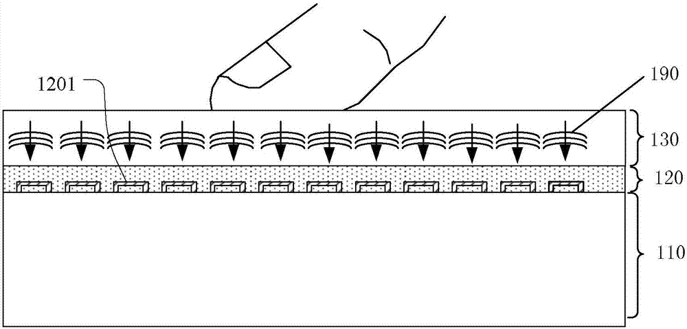
[0063] Figures 1a to 1c Shows how an ultrasonic sensor works. The ultrasonic sensor 100 includes a stacked CMOS circuit 110 , an ultrasonic transducer 120 , and a pressure plate 130 . The...


PUM


Abstract

The invention discloses an ultrasonic sensor and a manufacturing method thereof. The method comprises the steps of forming at least one ultrasonic transducer, forming a piezoelectric stack layer which comprises a piezoelectric layer, a firsts electrode and a second electrode which are respectively arranged on the first surface and the second surface of the piezoelectric layer, wherein the first layer and the second layer face each other; and forming an electric connection between the piezoelectric stack layer and a CMOS circuit, wherein the piezoelectric layer is composed of an organic piezoelectric polymer. According to the method, the piezoelectric layer is formed by the organic piezoelectric polymer, thereby reducing manufacture cost and improving sensor performance.

Description

technical field [0001] The present invention relates to biometric sensors, and more particularly, to ultrasonic sensors and methods of manufacturing the same. Background technique [0002] Biometric recognition is a technology used to distinguish different biological characteristics, including fingerprints, palm prints, faces, DNA, voice and other recognition technologies. Fingerprints refer to the uneven lines on the skin on the front of the end of a human finger, and the lines are regularly arranged to form different patterns. Fingerprint identification refers to identification by comparing the detailed feature points of different fingerprints. Due to its lifelong invariance, uniqueness and convenience, the application of fingerprint identification is more and more extensive. [0003] In fingerprint recognition, a sensor is used to obtain fingerprint image information. According to different working principles, fingerprint sensors can be divided into optical, capacitive...

Claims


Application Information

Patent Timeline
IPC IPC(8): G06K9/00
CPCG06V40/1306
Inventor 季锋闻永祥刘琛邹光祎
Owner HANGZHOU SILAN MICROELECTRONICS
Learn More