Array substrate, display panel, display apparatus and preparation method of array substrate

An array substrate and substrate substrate technology, which is applied in the manufacture of semiconductor/solid-state devices, electrical components, and electrical solid-state devices, etc., can solve the problems of increased power consumption of display devices, reduced brightness of display devices, and increased production costs, so as to reduce the display The effect of power consumption, reduction of process implementation requirements, and reduction of process cost

Active Publication Date: 2017-09-15
GUANG ZHOU NEW VISION OPTO ELECTRONICS TECH
View PDF3 Cites 8 Cited by
  • Summary
  • Abstract
  • Description
  • Claims
  • Application Information

AI Technical Summary

Problems solved by technology

However, since the subsequent addition of the color filter layer also requires the use of processes such as photolithography and alignment, this will increase the production process steps and process difficulty
Especially under the requirement of high pixel density display, the alignment accuracy of the color filter layer is very strict, which is not easy to achieve
More importantly, the introduction of the color filter layer will not only increase the production cost, but also greatly weaken the light output of the display device due to the existence of the color filter layer, which will reduce the brightness of the display device and cause the display device to fail when it is normally displayed. Increased consumption

Method used


Image

  • Array substrate, display panel, display apparatus and preparation method of array substrate
  • Array substrate, display panel, display apparatus and preparation method of array substrate
  • Array substrate, display panel, display apparatus and preparation method of array substrate

Examples


Embodiment Construction

[0025] The technical solutions of the present invention will be further described below in conjunction with the accompanying drawings and through specific implementation methods. It should be understood that the specific embodiments described here are only used to explain the present invention, but not to limit the present invention. In addition, it should be noted that, for the convenience of description, only some structures related to the present invention are shown in the drawings but not all structures.

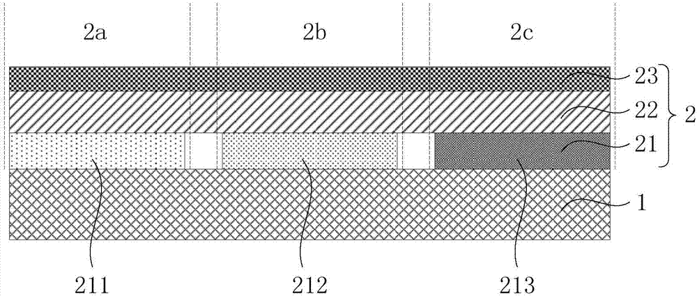
[0026] figure 1 It is a schematic structural diagram of an array substrate provided by an embodiment of the present invention. like figure 1 As shown, the array substrate includes:

[0027] substrate substrate 1;

[0028] A plurality of pixel units 2 are located on the base substrate 1, including a reflective electrode layer 21, a white light-emitting organic light-emitting layer 22 and a semi-transparent electrode layer 23 stacked in sequence; wherein, the white-lig...


PUM


Abstract

The invention discloses an array substrate, a display panel, a display apparatus and a preparation method of the array substrate. The array substrate comprises a substrate and multiple pixel units, wherein the multiple pixel units are positioned on the substrate and comprise a reflective electrode layer, a white light organic light emitting layer and a semi-transparent electrode layer; each pixel unit comprises a red sub pixel unit, a green sub pixel unit and a blue sub pixel unit; the reflective electrode layer comprises a first reflective electrode positioned on the red sub pixel unit, a second reflective electrode positioned on the green sub pixel unit and a third reflective electrode positioned on the blue sub pixel unit; the first reflective electrode has first reflective phase shifting on red light wavelength, the second reflective electrode has second reflective phase shifting on green light wavelength, and the third reflective electrode has third reflective phase shifting on blue light wavelength; and the first reflective phase shifting, the second reflective phase shifting and the third reflective phase shifting and the wavelengths of the corresponding emergent lights satisfy a Fabry-Perot resonance equation. The technological cost, display power consumption and technological realization requirement are lowered.

Description

technical field [0001] Embodiments of the present invention belong to the field of display technology, and relate to an array substrate, a display panel, a display device, and a method for preparing the array substrate. Background technique [0002] The technologies for realizing the colorization of Organic Light-Emitting Diode (OLED) include two mainstream technologies, that is, micro-cavity effect RGB pixel independent light-emitting technology, and white light-emitting materials combined with color filter layer technology. [0003] Micro-cavity effect RGB pixels need to use precision evaporation mask and pixel alignment technology to prepare red, green and blue primary color light-emitting centers of micro-cavity effect to achieve colorization, and precision evaporation mask is required. It is difficult to ensure the positioning accuracy of sub-pixels by using a precision evaporation mask, and it is difficult to achieve a display panel with high pixel density. Moreover, t...

Claims


Application Information

Patent Timeline
Patent Type & Authority Applications(China)
IPC IPC(8): H01L27/32H01L51/52H01L51/56
CPCH10K59/35H10K50/805H10K50/856H10K71/00
Inventor 高栋雨邹建华李洪濛徐苗王磊陶洪彭俊彪
Owner GUANG ZHOU NEW VISION OPTO ELECTRONICS TECH
Why Eureka
Try Eureka