


Quick Research
Generate reliable direction feasibility study reports for your R&D in just a few steps.

Technical Q&A
Discover and master advanced knowledge NOW. Basics, ideas, possibilities, all at once.

Find Solutions
As an expert in R&D theories, this can generate solutions to your technical problems instantly.

Evaluate Feasibility
Analyze your overall solution with one click, know your potential R&D risks in advance.

Monitor Landscape
Get weekly tech updates, stay abreast of the latest tech innovations and key insights.
Array substrate, preparation method of array substrate and display panel
An array substrate and display panel technology, applied in nonlinear optics, instruments, optics, etc., can solve the problems of light leakage of electrode lines and data lines, and achieve the effects of improving step difference, increasing size, and preventing light leakage
- Summary
- Abstract
- Description
- Claims
- Application Information
AI Technical Summary
Problems solved by technology
Method used
Image

Examples
Embodiment 1
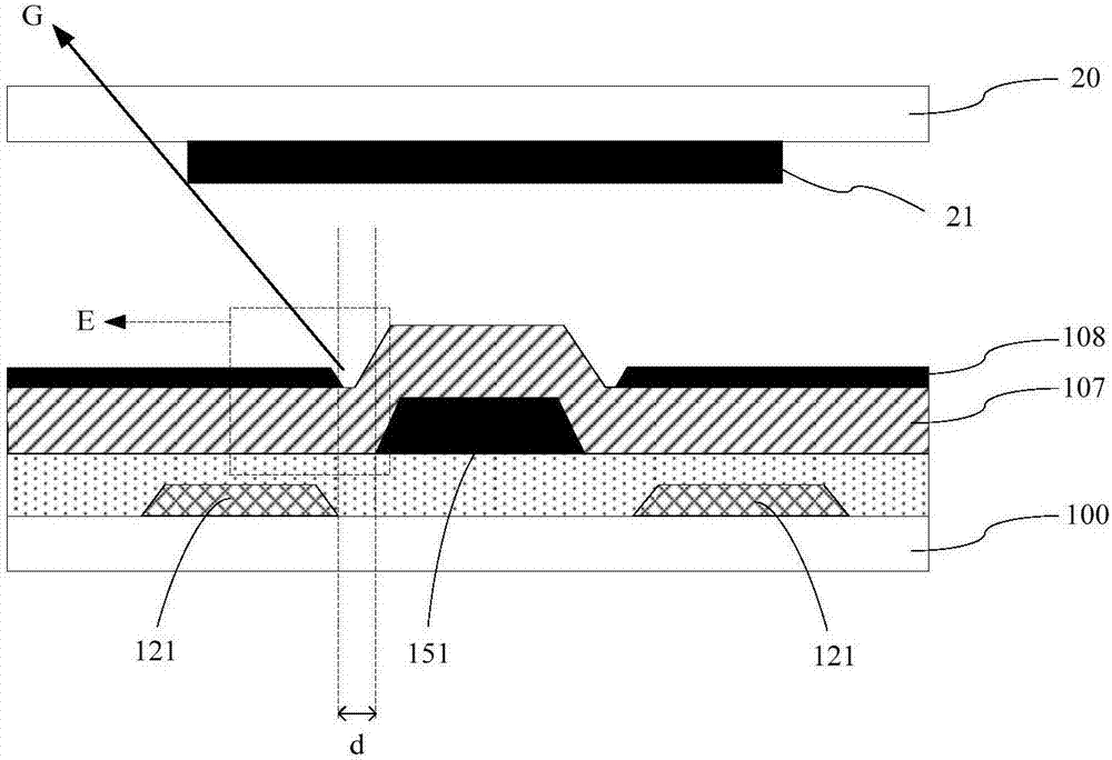
[0036] This embodiment provides an array substrate, such as Figure 6 As shown, it includes a substrate, the substrate is a glass substrate 100, on which storage capacitor electrode lines 121 are arranged, and an insulating layer 103 covering the storage capacitor electrode lines 121 is provided on the same layer as the insulating layer 103. The data line 151 and the light-shielding metal line 41 are insulated from each other, and the light-shielding metal line 41 is arranged on both sides of the data line 151 .
[0037]In the array substrate of this embodiment, mutually insulated data lines 151 and light-shielding metal lines 41 are arranged on the same layer on the insulating layer 103, so that even if the data lines 151 are shifted during the photolithography process, due to the existence of the light-shielding metal lines 41 Light leakage will occur; the light-shielding metal wire 41 on the insulating layer 103 is formed on both sides of the data line, which is equivalent ...
Embodiment 2
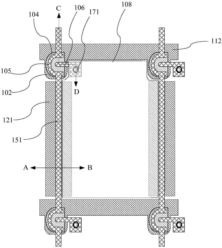
[0039] This embodiment provides an array substrate, such as Figure 7 As shown, it includes a substrate, the substrate is a glass substrate 100, two storage capacitor electrode lines 121 are arranged on the glass substrate 100, and an insulating layer 103 covering the storage capacitor electrode lines 121, the insulating layer 103 is on the same layer There are mutually insulated data lines 151 and two light-shielding metal lines 41, the two light-shielding metal lines 41 are arranged on both sides of the data line 151, the passivation layer 107 covers the data line 151 and the light-shielding metal lines 41, the passivation layer 107 A pixel electrode 108 is provided on it. Wherein, the orthographic projection of the data line 151 on the substrate has no overlapping area with the orthographic projection of the storage capacitor electrode line 121 on the substrate.
[0040] see Figure 7 For the sake of clarity, the diagrams all adopt a simplified drawing method, omit the fi...
Embodiment 3
[0053] This embodiment provides a method for preparing an array substrate, such as Figure 9 , Figure 10 Including the following preparation steps:
[0054] S01, using the glass substrate 100 as a substrate, forming storage capacitor electrode lines 121 thereon;
[0055] S02, forming an insulating layer 103 covering the storage capacitor electrode lines 121 on the substrate;
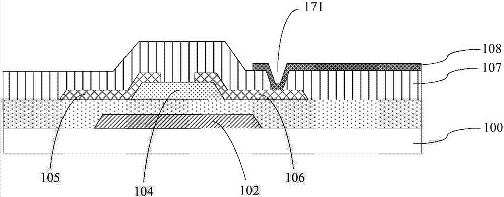
[0056] S03 , forming mutually insulated data lines 151 and light-shielding metal lines 41 on the insulating layer 103 by magnetron sputtering; wherein, the light-shielding metal lines 41 are disposed on both sides of the data line 151 .
[0057] Specifically, forming the mutually insulated data lines 151 and light-shielding metal lines 41 includes the following steps:
[0058] S03a, forming a first conductive layer 431 on the insulating layer 103; the first conductive layer 431 is a metal Al layer that is not easily etched by a dry method, and has a thickness of about 250 nm;
[0059] S03b, forming ...
PUM
| Property | Measurement | Unit |
|---|---|---|
| thickness | aaaaa | aaaaa |
| thickness | aaaaa | aaaaa |
Abstract
Description
Claims
Application Information
 - R&D Engineer
- R&D Manager
- IP Professional
- Industry Leading Data Capabilities
- Powerful AI technology
- Patent DNA Extraction
Browse by: Latest US Patents, China's latest patents, Technical Efficacy Thesaurus, Application Domain, Technology Topic, Popular Technical Reports.
© 2024 PatSnap. All rights reserved.Legal|Privacy policy|Modern Slavery Act Transparency Statement|Sitemap|About US| Contact US: help@patsnap.com