
Reflow-soldering die bonding process

A reflow soldering and reflow soldering technology, which is applied in the direction of assembling printed circuits with electric components, can solve the problems of reducing device reliability, increasing the thermal resistance of power MOS tubes, and increasing the on-resistance RDS, so as to reduce the generation of water vapor Effect

Active Publication Date: 2017-09-01
杭州晶志康电子科技有限公司
View PDF9 Cites 10 Cited by
  • Summary
  • Abstract
  • Description
  • Claims
  • Application Information

AI Technical Summary

Problems solved by technology

Among them, in the patch process, due to various factors, bubbles will be generated at the soldering place, and the existence of bubbles in the patch layer seriously affects the quality of the device, which can lead to excessive contact resistance and poor heat dissipation; it will also reduce the reliability of the device. properties, such as solder aging, intermetallic compound formation and delamination, eventually leading to chip cracking
The air bubbles will also increase the thermal resistance of the power MOS tube, causing the drift of many electrical parameters of the device, such as the increase of the on-resistance RDS, the drift of the threshold voltage, and the serious reduction of the safe working area of ​​the device.

Method used

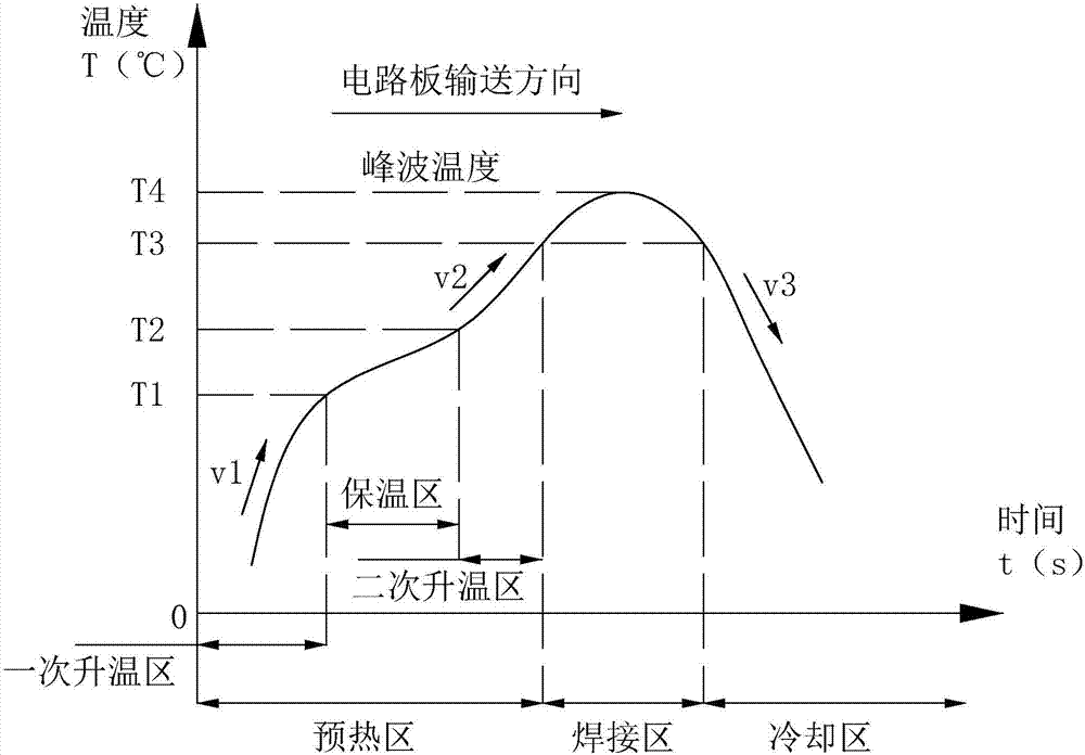
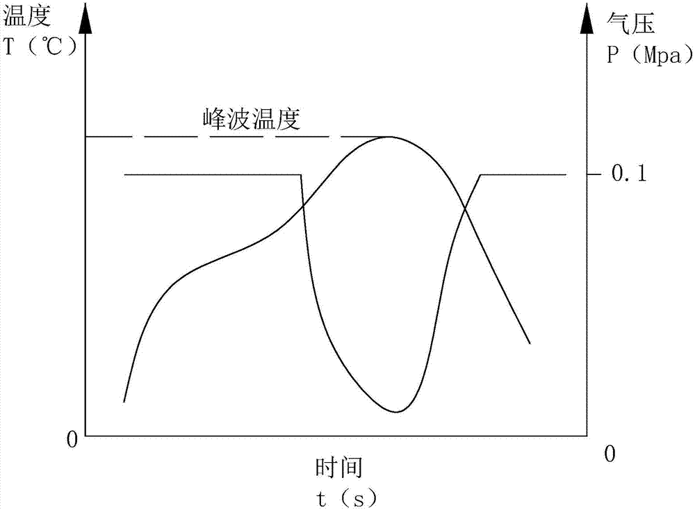
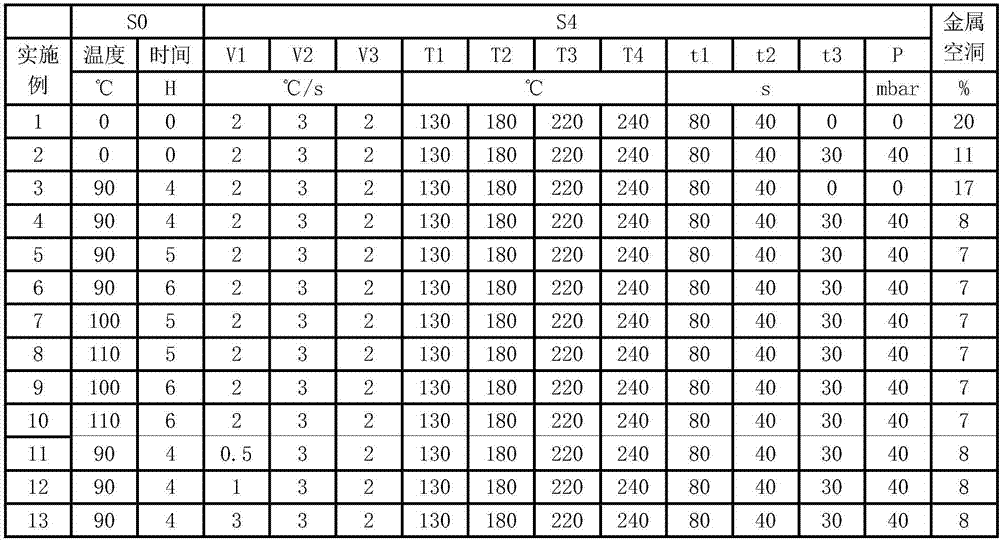

Image

  • Reflow-soldering die bonding process
  • Reflow-soldering die bonding process
  • Reflow-soldering die bonding process

Examples


Embodiment 1-56

[0036] Embodiment 1-56: A reflow soldering patch process, including the following steps:

[0037] S0. Drying, put the circuit board to be soldered into the oven for pre-bake 4-6H, the drying temperature is 90-110℃; S1, print the solder paste, check the circuit board with the optical camera, then put the circuit The board is pasted under the stencil, and while the lead-free scraper is moved above the stencil, the solder paste is printed on the circuit board through the mesh on the stencil. The solder paste is Sn-Ag-Cu series Alloy solder, in which the mesh holes of the steel mesh board are inverted tapered round holes to increase the surface area of ​​the solder paste printed on the circuit board;

[0038] S2, placement, send the circuit board after step S1 to the placement machine for placement;

[0039] S3. Intermediate inspection, check whether the polarity of the component is reversed, whether the mounting is offset, whether there is a short circuit, whether there are few or more...


PUM


Abstract

The invention discloses a reflow-soldering die bonding process. The process comprises the following steps of printing a solder paste, patching, intermediate inspection, reflow soldering and inspection after soldering. During the reflow soldering step, the pressure reduction treatment is conducted. In this way, the formation of cavities, due to the generation of huge air bubbles during the welding process, can be avoided. The formation of explosive exhausts, caused by the escaping of huge air bubbles, is also avoided. Since many fine tin beads are escaped, the negative pressure is formed in a welding zone through the pressure reduction treatment. Therefore, small air bubbles escape easily during the welding process, and huge air bubbles are not easily formed. The phenomenon of bead splashing is avoided.

Description

Technical field [0001] The invention relates to a circuit board patch technology, in particular to a reflow solder patch process. Background technique [0002] Due to the continuous miniaturization of electronic product circuit boards and the emergence of chip components, traditional welding methods can no longer meet the needs. With the development of surface mount technology, reflow soldering machines, which are part of surface mount technology, have also been developed accordingly, and their applications are becoming more and more extensive, and have been applied in almost all electronic product fields. A heater is provided in the soldering cavity formed in the soldering box of the reflow soldering machine, so that the circuit board components in the soldering cavity are welded together with the circuit board through the molten solder paste. [0003] Existing patch technology, such as an SMT patch process disclosed in a Chinese patent with the application publication number CN1...

Claims


Application Information

Patent Timeline
Patent Type & Authority Applications(China)
IPC IPC(8): H05K3/34
Inventor 王熠超
Owner 杭州晶志康电子科技有限公司
Learn More