
Liquid crystal display device and pixel structure thereof

A liquid crystal display device, pixel structure technology, applied in nonlinear optics, instruments, optics, etc., can solve problems such as dark lines, and achieve the effect of avoiding dark lines

Inactive Publication Date: 2017-08-15
HANNSTAR DISPLAY CORPORATION
View PDF5 Cites 1 Cited by
  • Summary
  • Abstract
  • Description
  • Claims
  • Application Information

AI Technical Summary

Problems solved by technology

However, the IPS liquid crystal display device and the FFS liquid crystal display device need to apply multi-field technology pixel structure to compensate for the color shift, and the current multi-field technology pixel structure is easy to cause dark lines

Method used


Image

  • Liquid crystal display device and pixel structure thereof
  • Liquid crystal display device and pixel structure thereof
  • Liquid crystal display device and pixel structure thereof

Examples


Embodiment Construction

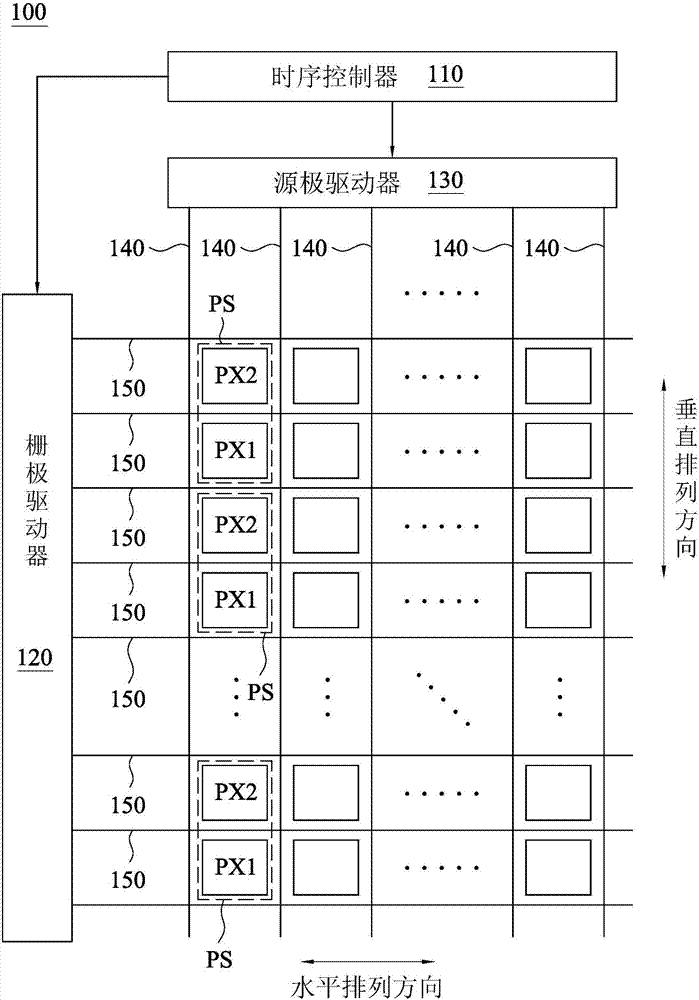
[0033] Please refer to figure 1 , figure 1 is a schematic diagram illustrating the structure of the liquid crystal display device 100 according to an embodiment of the present invention. The liquid crystal display device 100 includes a timing controller 110 , a gate driver 120 , a source driver 130 , a data line 140 , a scan line 150 and a pixel group PS. The timing controller 110 is used to control the gate driver 120 and the source driver 130 to provide data signals and scan signals to the data lines 140 and scan lines 150, wherein the data signals include pixel signals corresponding to each pixel, and the scan signals include Transistor switch signal corresponding to each pixel. The data lines 140 and the scan lines 150 are intersected with each other to define a plurality of pixel regions for setting pixels.

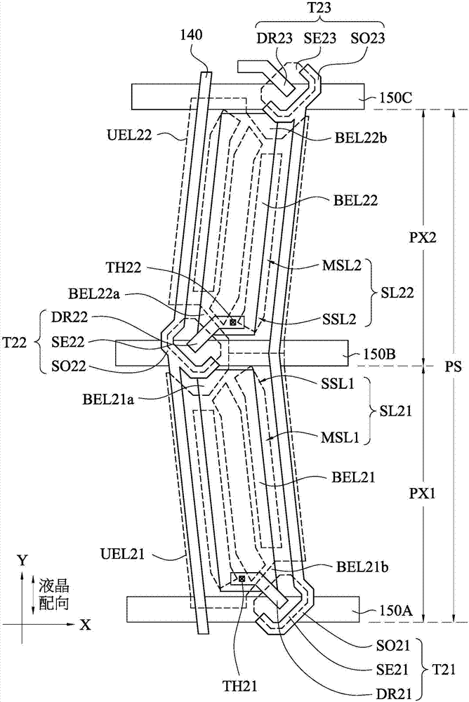
[0034] Each pixel group PS (one pixel structure) includes the first pixel PX1 (half pixel structure) and the second pixel PX2 (half pixel structure), and the firs...


PUM


Abstract

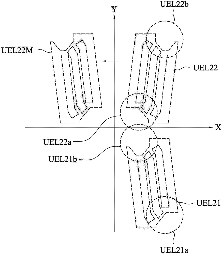
The invention discloses a liquid crystal display device and a pixel structure thereof. The pixel structure includes a first upper electrode, a first transistor, a second upper electrode, and a second transistor. The first upper electrode has a first pattern having a first end and a second end which are opposite to each other and at least one first slit. The first transistor is adjacent to the first end. The second upper electrode has a second pattern having a third end and a fourth end which are opposite to each other and at least one second slit. The third end is adjacent to the second end, and the fourth end is away from the second end. The second transistor is arranged between the second end and the third end. A mirror pattern generated by the second pattern of the second upper electrode according to a Y axis of an X-Y coordinate system is identical to the first pattern of the first upper electrode, and an X axis of the X-Y coordinate system is corresponding to the extension direction of a scanning line of the liquid crystal display device. Accordingly, the liquid crystal display device can avoid dark fringes.

Description

technical field [0001] The present invention relates to a liquid crystal display device and its pixel structure, and in particular relates to a liquid crystal display device and its pixel structure applying a multi-field pixel structure. Background technique [0002] With the current trend of multi-media applications tending to be diversified, the requirements for viewing angle and color performance of tablet computers, notebook computers or smart phones are becoming more and more stringent. In-Plane Switching (In Phase Switching; IPS) liquid crystal display devices and fringe field switching (Fringe Field Switching; FFS) liquid crystal display devices are currently technologies with the best viewing angle and color performance. Since the IPS liquid crystal display device and the FFS liquid crystal display device are driven by a horizontal electric field, they have little dependence on the viewing angle. Compared with other types of liquid crystal display devices, such as t...

Claims


Application Information

Patent Timeline
Patent Type & Authority Applications(China)
IPC IPC(8): G02F1/1343
CPCG02F1/134309G02F1/134318G02F1/134372
Inventor 郭丰玮高翎志李昆政
Owner HANNSTAR DISPLAY CORPORATION
Learn More