Vacuum lamination method and device for tsv process and bonding system using same

A technology of vacuum layer and process, which is applied in the direction of lamination equipment, lamination, chemical instruments and methods, etc. It can solve the problems of complex lamination, bonding and debonding process, difficult maintenance, management and repair, complex and large-scale equipment, etc. problems, to achieve the effects of suppressing voids, saving maintenance and management costs, and simplifying process layout

Active Publication Date: 2020-11-20
AP SYST INC
View PDF2 Cites 0 Cited by
  • Summary
  • Abstract
  • Description
  • Claims
  • Application Information

AI Technical Summary

Problems solved by technology

[0014] Also, in the past, peeling was performed on the upper side of the temporary adhesive film, so that particles fell on the peeled temporary adhesive film, resulting in a decrease in lamination quality
[0015] In addition, the overall process layout in the past is very complicated for supplying, cutting and peeling the temporary adhesive film, arranging it, and then laminating, bonding and debonding the carrier wafer, which also makes the device complicated. , large-scale, which makes it difficult to maintain, manage and repair, and the efficiency of the entire process is low, which leads to a decrease in throughput

Method used


Image

  • Vacuum lamination method and device for tsv process and bonding system using same
  • Vacuum lamination method and device for tsv process and bonding system using same
  • Vacuum lamination method and device for tsv process and bonding system using same

Examples


Embodiment Construction

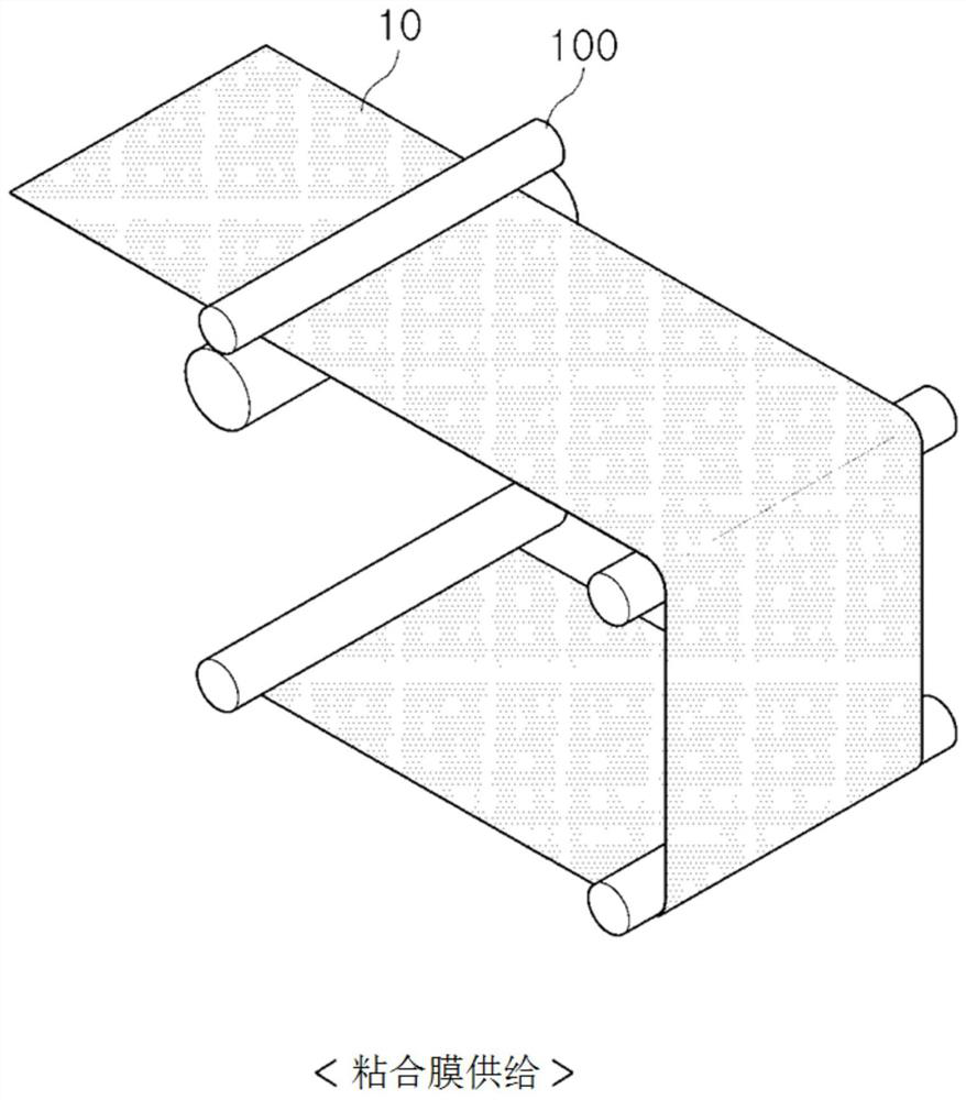
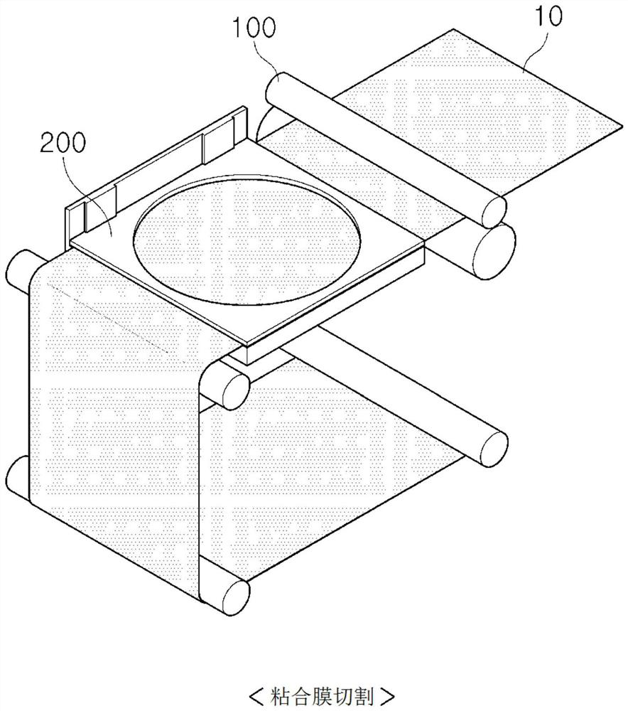
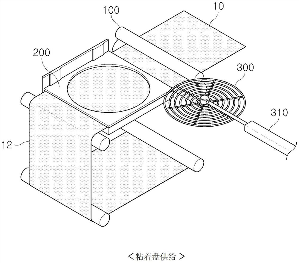
[0036] The present invention relates to a lamination process of a through-silicon via (Through Silicon Via, hereinafter referred to as "TSV") process for improving the integration degree of semiconductor elements.

[0037] In particular, an adhesive film capable of efficiently laminating an adhesive film to a carrier wafer for maintaining the strength of a device wafer relates to a vacuum lamination for high-quality vacuum lamination capable of suppressing generation of dust and particles.

[0038] Figure 1 to Figure 8 is a schematic diagram of the vacuum lamination process sequence and the main parts of the device according to the present invention, Figure 9 to Figure 11 is a diagram illustrating an example of a bonding system according to vacuum lamination in the present invention.

[0039] As shown in the figure, the adhesive film 10 and the carrier wafer 20 are laminated in a vacuum state in the present invention, so generation of dust and particles can be minimized, th...


PUM


Abstract

The present invention relates to a laminating method for TSV process, comprising: an adhesive film supplying step of supplying the adhesive film with a transfer roller; an adhesive film cutting step of cutting the adhesive film into a prescribed shape with a cutter; the first The step of peeling the protective film, sticking the adhesive film cut into the prescribed shape to the lower part of the adhesive disc, and peeling the first protective film formed on the lower part of the adhesive film; the step of separating the adhesive disc, the first protective film After the peeled adhesive film is transferred to a vacuum laminator through the adhesive tray and placed on the carrier wafer, the adhesive tray is separated from the adhesive film; the vacuum lamination step, for placement on the carrier wafer laminating the adhesive film and the carrier wafer; and a second protective film peeling step of peeling the second protective film formed on the upper part of the adhesive film. Thereby, the adhesive film and the carrier wafer are laminated in a vacuum state to minimize generation of dust and particles, and high-quality lamination can be realized.

Description

technical field [0001] The invention is used to implement a lamination process for a through silicon via (TSV, through silicon via) process, and relates to a vacuum lamination method for a TSV process, a vacuum laminating apparatus (vacuum laminating apparatus) for a TSV process, and bonding using the same The system, the above method, apparatus and system can perform lamination of an adhesive film and a carrier wafer in a vacuum state, thereby minimizing generation of dust and particles, thereby enabling high-quality lamination. Background technique [0002] So far, researches on improving the integration degree of semiconductor devices have been continuously carried out. However, due to the physical limitations of exposure devices used to form circuit patterns, researchers in the field are faced with the difficult reality that they cannot further improve the integration level with existing equipment and methods. [0003] Recently, some new technologies that can improve th...

Claims


Application Information

Patent Timeline
Patent Type & Authority Patents(China)
IPC IPC(8): B32B37/10B32B37/12H01L21/67
CPCH01L21/67132H01L21/6836H01L2221/68327H01L2221/68386Y02P70/50H01L24/26H01L21/022H01L2224/03436
Inventor 李锡政徐城泽韩宰贤
Owner AP SYST INC
Why Eureka
Try Eureka