Fully differential amplifier and its residual gain circuit
A fully differential amplifier and differential input technology, applied in the direction of differential amplifiers, amplifiers, amplification control, etc., can solve the problems of low power consumption, gain reduction, gain high speed, etc., achieve fast charge and discharge characteristics, and improve DC gain , the effect of increasing the equivalent gain
- Summary
- Abstract
- Description
- Claims
- Application Information
AI Technical Summary
Problems solved by technology
Method used
Image
Examples
Embodiment 1
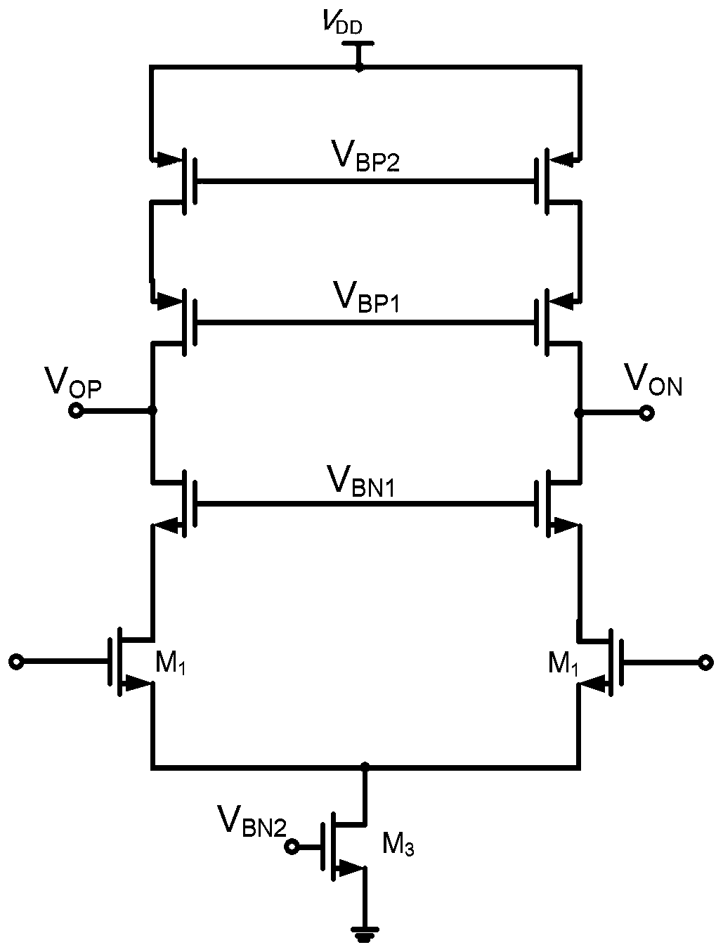
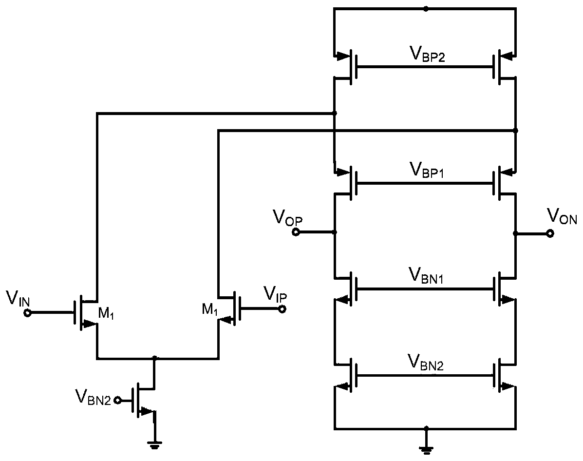
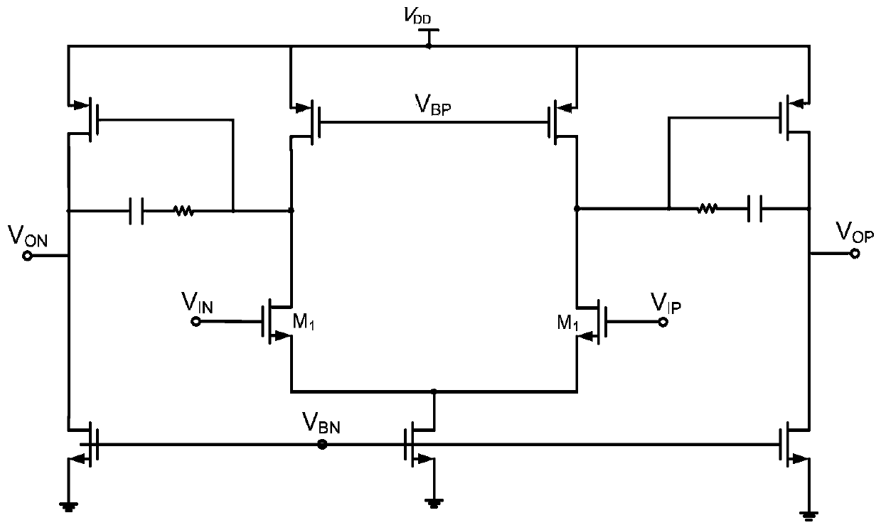
[0052] Such as Figure 4 As shown, this embodiment proposes a fully differential amplifier, including a first complementary differential input pair 101, a second complementary differential input pair 102, and all connected to the first complementary differential input pair 101 and the second complementary differential input pair 102 The first tail current source 104 and the second tail current source 105, the fully differential amplifier also includes a positive feedback system 103, connected with the first complementary differential input pair 101 and the second complementary differential input pair 102, for providing the first complementary differential input pair The input pair 101 and the second complementary differential input pair 102 provide positive feedback.
[0053] Specifically, the first complementary differential input pair 101 has two equal-sized and complementary MOS transistors M1A and M1B, and the gates of the two MOS transistors M1A and M1B are connected to t...
Embodiment 2
[0062] Such as Figure 6 As shown, this embodiment proposes a residual gain circuit (MDAC), which uses the fully differential amplifier in Embodiment 1 (see Figure 6 The structure inside the dotted line frame), and introduces the CLS technology to improve the equivalent gain of the amplifier. C1 and C2 are sampling capacitors of the same size, and the output of MDAC can achieve 2V IN -V DAC , where V IN is the input voltage, V DAC is the output voltage of the sub-digital-to-analog converter (Sub-DAC).
[0063] Since when the output of the amplifier reaches the maximum swing, the third complementary differential input pair M3A and M3B of the positive feedback system may enter the linear region, which will cause the gain of the amplifier to drop. However, with the help of the CLS method, the final output of the amplifier can always be stable at the common-mode output level V CM Nearby, the gain of the amplifier is maintained, thereby reducing the gain nonlinearity.
[00...
PUM
 Abstract
Description
Claims
Application Information
 - R&D
- Intellectual Property
- Life Sciences
- Materials
- Tech Scout
- Unparalleled Data Quality
- Higher Quality Content
- 60% Fewer Hallucinations
Browse by: Latest US Patents, China's latest patents, Technical Efficacy Thesaurus, Application Domain, Technology Topic, Popular Technical Reports.
© 2025 PatSnap. All rights reserved.Legal|Privacy policy|Modern Slavery Act Transparency Statement|Sitemap|About US| Contact US: help@patsnap.com


