Static chuck mechanism and semiconductor processing equipment

An electrostatic chuck and electrostatic heating technology, which is applied in the direction of metal processing equipment, semiconductor/solid-state device manufacturing, metal processing machinery parts, etc., can solve the problem of uneven temperature in the edge area and center area of ​​the wafer, the inability of the heater to control the temperature, and the inability to meet Etching uniformity and other issues to achieve the effect of improving process uniformity and heat transfer effect

Inactive Publication Date: 2017-06-27
BEIJING NAURA MICROELECTRONICS EQUIP CO LTD
View PDF4 Cites 7 Cited by
  • Summary
  • Abstract
  • Description
  • Claims
  • Application Information

AI Technical Summary

Problems solved by technology

Yet due to being limited by the physical size of the electrostatic chuck 8, the heater in the electrostatic chuck 8 cannot control the temperature of the wafer near its edge (because the diameter of the wafer 5 is slightly larger than the outer diameter of the electrostatic chuck 8, the heater It is impossible to control the temperature of the part of the periphery of the wafer 5 that is not in contact with the electrostatic chuck 8), resulting in uneven temperatures in the edge area and the center area of ​​the wafer, which cannot meet the etching requirements for the edge area and the center area of ​​the wafer in 28-20 nanometer technology uniformity requirements

Method used


Image

  • Static chuck mechanism and semiconductor processing equipment
  • Static chuck mechanism and semiconductor processing equipment
  • Static chuck mechanism and semiconductor processing equipment

Examples


Embodiment Construction

[0024] In order for those skilled in the art to better understand the technical solutions of the present invention, the electrostatic chuck mechanism and semiconductor processing equipment provided by the present invention will be described in detail below in conjunction with the accompanying drawings.

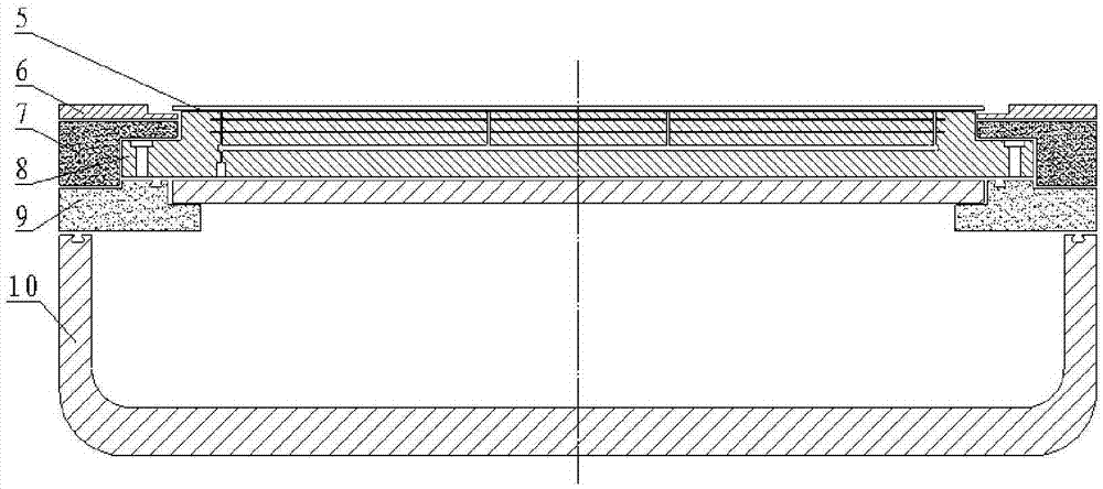
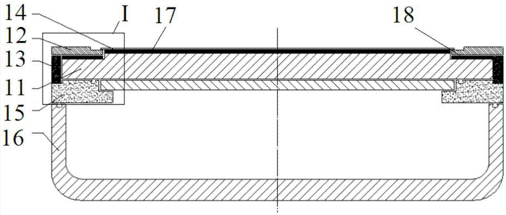
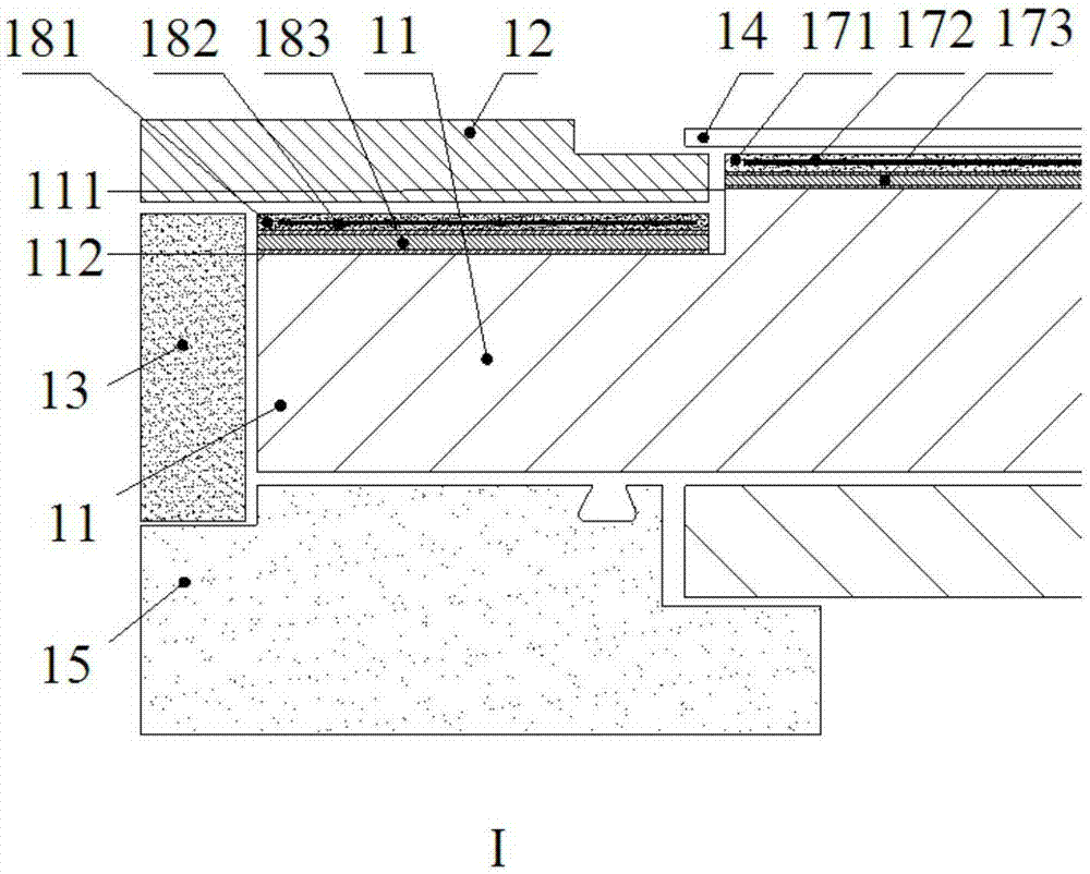
[0025] figure 2 A cross-sectional view of an electrostatic chuck mechanism provided by an embodiment of the present invention. image 3 for figure 2 Zoom-in view of the middle I region. Please also refer to figure 2 with image 3 , the electrostatic chuck mechanism includes a base 11 , an edge component, a main body electrostatic heating layer 17 and an edge electrostatic heating layer 18 . Wherein, the base 11 includes a carrying surface 111 for carrying the wafer 14 , and a stepped surface 112 surrounding the carrying surface 111 and located at an edge of the wafer 14 , and the stepped surface 112 is lower than the carrying surface 111 . That is to say, a boss is for...


PUM


Abstract

The invention provides a static chuck mechanism and semiconductor processing equipment. The mechanism comprises a substrate, an edge assembly, a main static heating layer and an edge static heating layer. The substrate comprises a bearing surface for bearing a wafer, a stepped surface which surrounds the periphery of the bearing surface and is located at the edge of the wafer and is lower than the bearing surface. The edge assembly comprises a focusing ring, a base ring and an insulating ring, wherein the focusing ring is disposed on the stepped surface in a surrounding manner. The insulating ring is disposed at the bottom of the substrate, and supports the substrate. The main static heating layer is disposed on the bearing surface, and is used for the electrostatic absorption of the wafer, and the adjustment of the temperature of the wafer. The edge static heating layer is disposed on the stepped surface, and is used for the electrostatic absorption of the focusing ring and the adjustment of the temperature of the focusing ring. The mechanism provided by the invention can independently adjust the temperature of the central region and edge region of the wafer, can achieve the compensation for the temperature difference between the edge region and the central region of the wafer, and can improve the technological uniformity.

Description

technical field [0001] The invention relates to the field of semiconductor equipment manufacturing, in particular to an electrostatic chuck mechanism and semiconductor processing equipment. Background technique [0002] In the process of manufacturing integrated circuits (IC) and microelectromechanical systems (MEMS), especially in the process of implementing plasma etching (ETCH), physical vapor deposition (PVD), chemical vapor deposition (CVD), etc., often The electrostatic chuck is used to carry and heat the wafer and other processed workpieces, provide DC bias voltage for the wafer and control the temperature of the wafer surface. [0003] figure 1 It is a schematic structural diagram of a typical electrostatic chuck mechanism. Such as figure 1 As shown, the electrostatic chuck mechanism includes an electrostatic chuck 8 and an edge assembly. Wherein, the electrostatic chuck 8 is used to fix the wafer 5 on its upper surface by means of electrostatic adsorption, and a...

Claims


Application Information

Patent Timeline
Patent Type & Authority Applications(China)
IPC IPC(8): H01L21/683H01L21/67
CPCH01L21/67011H01L21/67098H01L21/6831H01J37/32H01L21/67103H01L21/67109H01L21/6833B23Q3/15H01L21/67248H01L21/6835H01L21/68721H02N13/00H01L21/4871
Inventor 彭宇霖
Owner BEIJING NAURA MICROELECTRONICS EQUIP CO LTD
Why Eureka
Try Eureka