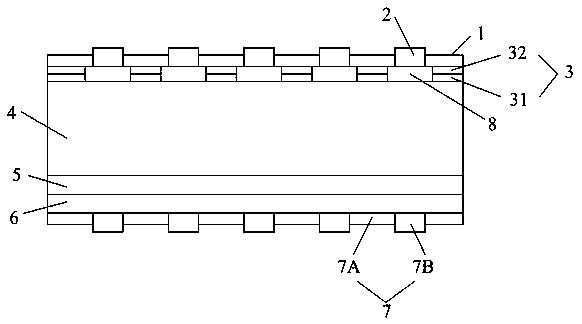
P-type perc bifacial solar cell, component, system and preparation method thereof
A solar cell and double-sided technology, applied in the field of solar cells, can solve the problems of complex N-type double-sided cell process and high price of N-type silicon wafers, and achieve the effect of improving photoelectric conversion efficiency, high photoelectric conversion efficiency and low cost
- Summary
- Abstract
- Description
- Claims
- Application Information
AI Technical Summary
Problems solved by technology
Method used
Image
Examples
Embodiment approach
[0070] It should be noted that there are various implementations of the laser groove unit 81, including:
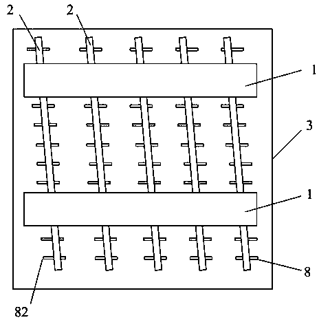
[0071] (1) Each group of laser grooving units 81 includes a laser grooving body 82. At this time, the laser grooving unit 81 is a continuous linear grooving area, specifically as Figure 5 shown. Multiple laser grooving units 81 are arranged vertically.
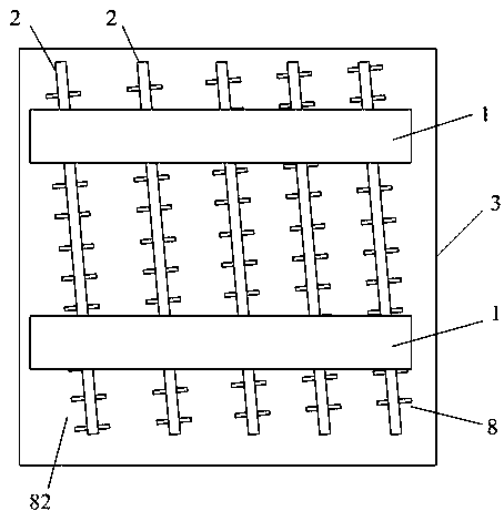
[0072] (2) Each group of laser grooving units 81 includes a plurality of laser grooving bodies 82. At this time, the laser grooving units 81 are line-segment non-continuous linear grooving areas, specifically as Figure 4 shown. The plurality of laser grooved bodies 82 may be two, three, four or more, but not limited thereto. Multiple laser grooving units 81 are arranged vertically.
[0073] When each group of laser grooving units 81 includes a plurality of laser grooving bodies 82, it is divided into the following situations:
[0074] A. The width, length and shape of multiple laser grooved bodies 82 are the same, ...
Embodiment 1
[0111] (1) Form a suede surface on the front and back of the silicon wafer, and the silicon wafer is P-type silicon;
[0112] (2) Diffusion of the silicon wafer to form an N-type emitter;
[0113] (3) Remove the front phosphosilicate glass and surrounding PN junctions formed during the diffusion process;
[0114] (4) Deposit aluminum oxide film on the back of the silicon wafer;
[0115] (5) Deposit a silicon nitride film on the back of the silicon wafer;
[0116] (6) Deposit a silicon nitride film on the front side of the silicon wafer;
[0117] (7) Laser grooving the back of the silicon wafer to form a laser grooving area. The laser grooving area includes multiple sets of laser grooving units arranged in the horizontal direction, each group of laser grooving units includes a laser grooving unit arranged in the horizontal direction. Groove body, the length of the laser grooved body is 1000 microns, and the width is 40 microns;
[0118] (8) printing a back silver busbar ele...
Embodiment 2
[0124] (1) Form a suede surface on the front and back of the silicon wafer, and the silicon wafer is P-type silicon;
[0125] (2) Diffusion of the silicon wafer to form an N-type emitter;
[0126] (3) Remove the front phosphosilicate glass and surrounding PN junctions formed by the diffusion process, and polish the back of the silicon wafer;
[0127] (4) Deposit aluminum oxide film on the back of the silicon wafer;
[0128] (5) Deposit a silicon nitride film on the back of the silicon wafer;
[0129] (6) Deposit a silicon nitride film on the front side of the silicon wafer;
[0130] (7) Laser grooving the back of the silicon wafer to form a laser grooving area, the laser grooving area includes multiple sets of obliquely arranged laser grooving units, and each group of laser grooving units includes multiple obliquely arranged laser grooving units Body, the length of the laser grooved body is 500 microns, and the width is 50 microns;
[0131] (8) printing a back silver busba...
PUM
| Property | Measurement | Unit |
|---|---|---|
| length | aaaaa | aaaaa |
| width | aaaaa | aaaaa |
| thickness | aaaaa | aaaaa |
Abstract
Description
Claims
Application Information
 - R&D
- Intellectual Property
- Life Sciences
- Materials
- Tech Scout
- Unparalleled Data Quality
- Higher Quality Content
- 60% Fewer Hallucinations
Browse by: Latest US Patents, China's latest patents, Technical Efficacy Thesaurus, Application Domain, Technology Topic, Popular Technical Reports.
© 2025 PatSnap. All rights reserved.Legal|Privacy policy|Modern Slavery Act Transparency Statement|Sitemap|About US| Contact US: help@patsnap.com


