Display panel, manufacturing method thereof, and display device

A technology of a display panel and a manufacturing method, which is applied in the directions of instruments, nonlinear optics, optics, etc., can solve the problems of reduced display quality, large overlapping area between data lines and common electrodes, and greenishness.

Active Publication Date: 2020-07-10
BOE TECH GRP CO LTD +1
View PDF6 Cites 0 Cited by
  • Summary
  • Abstract
  • Description
  • Claims
  • Application Information

AI Technical Summary

Problems solved by technology

However, in the HADS type liquid crystal display, the overlapping area of ​​the data line and the common electrode is relatively large, so the parasitic capacitance generated between the data line and the common electrode is relatively large
Therefore, affected by the parasitic capacitance RC delay, the common voltage in the panel will attenuate as the distance from the common voltage input terminal increases, resulting in a smaller common voltage charged to the common electrode in the area farther from the common voltage input terminal. , so that the phenomenon of greenish (Greenish) in the above-mentioned areas during the display process is more serious
And with the improvement of resolution, the above-mentioned green phenomenon will become more and more serious, thereby reducing the display quality

Method used


Image

  • Display panel, manufacturing method thereof, and display device
  • Display panel, manufacturing method thereof, and display device
  • Display panel, manufacturing method thereof, and display device

Examples


Embodiment Construction

[0034]The following will clearly and completely describe the technical solutions in the embodiments of the present invention with reference to the accompanying drawings in the embodiments of the present invention. Obviously, the described embodiments are only some, not all, embodiments of the present invention. Based on the embodiments of the present invention, all other embodiments obtained by persons of ordinary skill in the art without making creative efforts belong to the protection scope of the present invention.

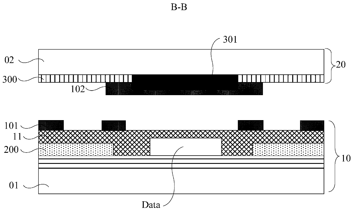
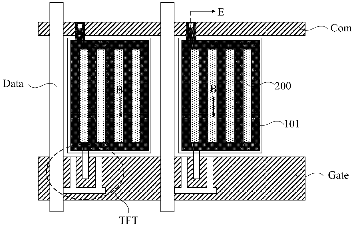
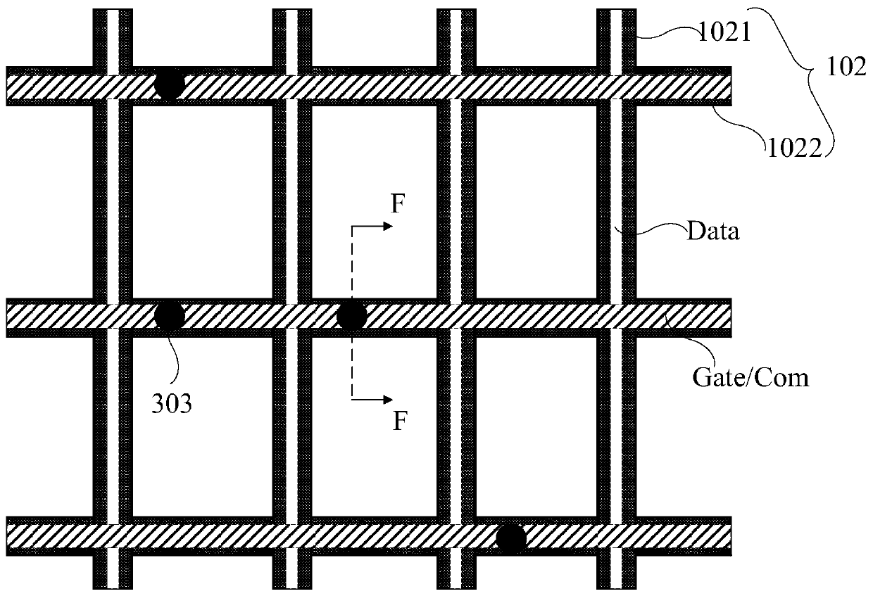
[0035] An embodiment of the present invention provides a display panel, such as figure 1 As shown, it includes a first substrate 10 and a second substrate 20 disposed opposite to each other. Wherein, the first substrate 10 has a first common electrode 101 and a pixel electrode 200 arranged in different layers. The first common electrode 101 is closer to the second substrate 20 than the pixel electrode 200 . In addition, the orthographic projection of the firs...


PUM


Abstract

Embodiments of the present invention provide a display panel, a manufacturing method thereof, and a display device, which relate to the field of display technology and can reduce parasitic capacitance between a common electrode and a data line. The display panel includes a first substrate and a second substrate oppositely arranged. The first common electrode and the pixel electrode are arranged in different layers on the first substrate, and the first common electrode is closer to the second substrate than the pixel electrode. A second common electrode is provided on the second substrate, and the second common electrode is electrically connected to the first common electrode. The orthographic projection of the second common electrode on the first substrate has an overlapping area with the data line on the first substrate, and the orthographic projection of the first common electrode on the first substrate has no overlapping area with the data line. The display panel is used to display images.

Description

technical field [0001] The present invention relates to the field of display technology, in particular to a display panel, a manufacturing method thereof, and a display device. Background technique [0002] TFT-LCD (Thin Film Transistor Liquid Crystal Display, Thin Film Transistor Liquid Crystal Display), as a flat panel display device, has become more and more popular due to its small size, low power consumption, no radiation and relatively low production cost. It is widely used in the field of high-performance display. [0003] The TFT-LCD is provided with a pixel electrode and a common electrode, and by controlling the magnitude of the electric field generated by the pixel electrode and the common electrode, the purpose of controlling the deflection direction of the liquid crystal is achieved. In order to increase the pixel aperture ratio, those skilled in the art have proposed a high aperture ratio Advanced Super Dimensional Switching (High Aperture Advanced Super Dimen...

Claims


Application Information

Patent Timeline
Patent Type & Authority Patents(China)
IPC IPC(8): G02F1/1343G02F1/1339G02F1/1335
CPCG02F1/133512G02F1/1339G02F1/13394G02F1/134309G02F1/136286G02F1/134318G02F1/134372G02F1/13398G02F1/134381G02F1/136295G02F1/134363G02F1/136209G02F2201/121G02F2201/123
Inventor 刘海峰马小叶马睿
Owner BOE TECH GRP CO LTD
Why Eureka
Try Eureka