Polar plate structure, electrostatic driving structure utilizing polar plate structure and manufacturing method thereof
A plate structure, electrostatic drive technology, applied in microstructure technology, microstructure devices, manufacturing microstructure devices, etc., can solve problems such as etching damping holes, and achieve the effect of easy preparation and large electrostatic force/damping force ratio
- Summary
- Abstract
- Description
- Claims
- Application Information
AI Technical Summary
Problems solved by technology
Method used
Image
Examples
Embodiment 1
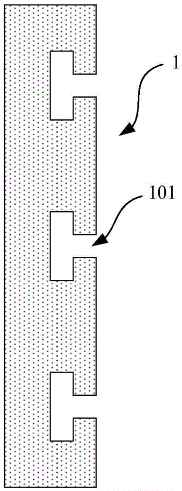
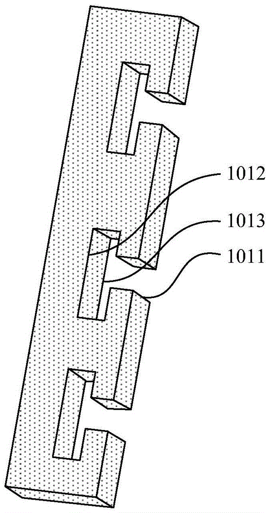
[0056] The invention provides a plate structure, please refer to figure 2 and image 3 , Respectively shown as a top view and a three-dimensional view of the electrode plate structure 1. As shown in the figure, one side of the electrode plate structure 1 is provided with at least one damping hole 101 that penetrates the electrode plate structure 1 up and down, wherein the damping The openings of the holes 101 on the side, upper and lower surfaces of the electrode plate structure are side openings 1011, upper openings 1012, and lower openings 1013, respectively, and the area of the upper opening 1012 or the area of the lower opening 1013 is larger than that of the lower opening 1013. The area of the side opening 1011 is described.
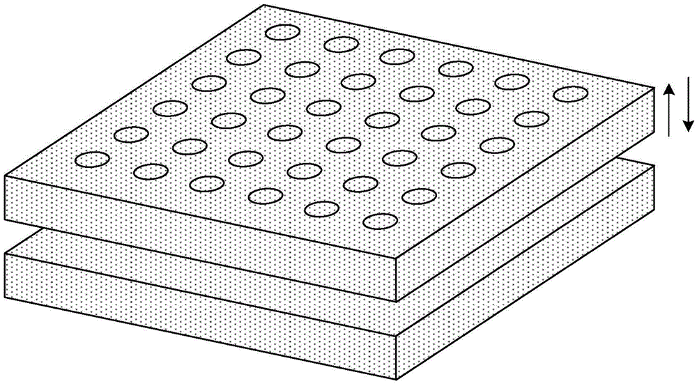
[0057] Such as Figure 4 As shown, it is a schematic diagram showing the relative movement of two movable parts adopting the pole plate structure of the present invention in a plane. The relative movement in the plane here refers to the relative...
Embodiment 2
[0065] The present invention also provides a manufacturing method of the electrode structure, which includes the following steps:
[0066] Such as Picture 11 As shown, step S1 is performed: a substrate 201 is provided, a cavity structure 203 is etched in the substrate 201, and an insulating layer 202 is formed on the surface of the cavity structure 203.
[0067] Specifically, the substrate 201 includes, but is not limited to, conventional semiconductor materials such as Si, Ge, and SiGe. The insulating layer 202 includes but is not limited to compound materials such as silicon oxide and silicon nitride. In this embodiment, the substrate 201 is an Si substrate, and the insulating layer 202 is silicon oxide.
[0068] The cavity structure 203 can be obtained by dry etching or wet etching. The function of the cavity structure 203 is to provide a floating space for the subsequent formation of a suspended electrode structure, and its shape is not limited.
[0069] Such as Picture 12 As ...
Embodiment 3
[0078] The present invention also provides an electrostatic drive structure adopting the pole plate structure of any one of the embodiments.
[0079] Specifically, the electrostatic drive structure includes a movable electrode and a fixed electrode, and the movable electrode and the fixed electrode may be a flat electrode or an interdigital electrode.
[0080] As an example, the movable electrode and the fixed electrode move relative to each other in the same plane, and at least one of the movable electrode and the fixed electrode adopts the electrode plate structure, that is, there may be only a movable electrode The electrode plate structure of the present invention is adopted, or only the fixed electrode adopts the electrode plate structure of the present invention, or both the movable electrode and the fixed electrode adopt the electrode plate structure of the present invention.
[0081] As an example, such as Figure 15 As shown, it shows an electrostatic drive structure 3 using...
PUM
 Abstract
Description
Claims
Application Information
 - Generate Ideas
- Intellectual Property
- Life Sciences
- Materials
- Tech Scout
- Unparalleled Data Quality
- Higher Quality Content
- 60% Fewer Hallucinations
Browse by: Latest US Patents, China's latest patents, Technical Efficacy Thesaurus, Application Domain, Technology Topic, Popular Technical Reports.
© 2025 PatSnap. All rights reserved.Legal|Privacy policy|Modern Slavery Act Transparency Statement|Sitemap|About US| Contact US: help@patsnap.com


